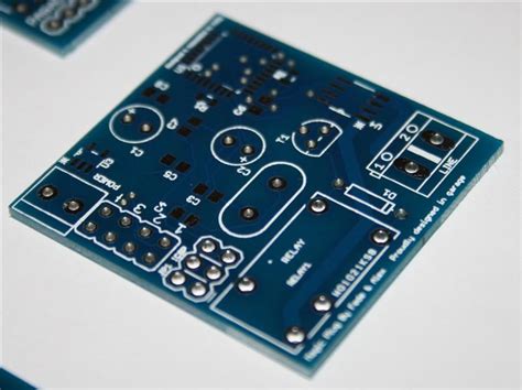
Introduction to DIY PCB
Printed Circuit Boards (PCBs) are the backbone of modern electronics. They are used in almost every electronic device, from smartphones and computers to home appliances and industrial equipment. PCBs provide a way to mechanically support and electrically connect electronic components using conductive pathways, tracks, or signal traces etched from copper sheets laminated onto a non-conductive substrate.
While PCBs are typically manufactured in large quantities by specialized companies, it is also possible to create your own PCBs at home. DIY PCB (Do-It-Yourself Printed Circuit Board) is a process of designing, fabricating, and assembling PCBs in a home or small workshop setting. This can be a fun and rewarding hobby for electronics enthusiasts, as well as a cost-effective way to prototype and test new designs.
Benefits of DIY PCB
- Cost-effective for small-scale projects and prototypes
- Faster turnaround time compared to ordering from a manufacturer
- Ability to customize and iterate on designs quickly
- Opportunity to learn about PCB design and fabrication processes
- Satisfaction of creating something from scratch
Tools and Materials Needed for DIY PCB
To get started with DIY PCB, you will need a few essential tools and materials. Here is a list of the basic items you will need:
Hardware
- PCB material (copper-clad board)
- Drill or drill press
- Dremel tool or hand drill
- Soldering iron and solder
- Multimeter
- Safety glasses and gloves
Chemicals
- Ferric chloride or other etchant solution
- Acetone or isopropyl alcohol for cleaning
- Photoresist or UV-sensitive film
- Developer solution
Software
- PCB design software (e.g., KiCad, Eagle, Altium Designer)
- Gerber file viewer
- CAM processor

Step-by-Step Guide to Making a DIY PCB
Now that you have gathered all the necessary tools and materials, let’s dive into the step-by-step process of creating a DIY PCB.
Step 1: Design your PCB
The first step in creating a DIY PCB is to design your circuit using PCB design software. There are many options available, both free and paid, such as KiCad, Eagle, and Altium Designer. Choose the software that best suits your needs and skill level.
When designing your PCB, keep in mind the following considerations:
- Component placement and orientation
- Track width and spacing
- Via size and placement
- Ground planes and power planes
- Silkscreen labels and markings
Step 2: Print your PCB design
Once you have completed your PCB design, you need to print it onto a transparency or photoresist film. This will be used to transfer the design onto the copper-clad board.
If using a transparency, print your design onto the film using a laser printer. Make sure the design is printed as a mirror image, as it will be flipped when transferred onto the board.
If using photoresist film, follow the manufacturer’s instructions for exposing and developing the film.
Step 3: Transfer the design onto the copper-clad board
With your printed design ready, it’s time to transfer it onto the copper-clad board. Here’s how to do it:
- Clean the copper-clad board with acetone or isopropyl alcohol to remove any dirt or grease.
- Place the printed transparency or developed photoresist film onto the copper side of the board, ensuring it is aligned correctly.
- Secure the film in place using tape or a glass plate.
- Expose the board to UV light for the recommended time (usually a few minutes).
- Remove the film and develop the board using the appropriate developer solution.
- Rinse the board with water and dry it thoroughly.
Step 4: Etch the PCB
Now that your design is transferred onto the copper-clad board, it’s time to etch away the unwanted copper. The most common method is to use ferric chloride solution, which can be purchased from electronics suppliers or online.
- Put on safety glasses and gloves before handling the etchant solution.
- Pour the ferric chloride solution into a non-metallic container, such as a plastic tray.
- Immerse the PCB into the solution, copper side facing up.
- Agitate the solution gently to ensure even etching.
- Check the progress every few minutes until all the unwanted copper is removed.
- Remove the board from the solution and rinse it thoroughly with water.
- Clean the board with acetone or isopropyl alcohol to remove any remaining photoresist.
Step 5: Drill holes and cut out the PCB
With the etching complete, you need to drill holes for the components and cut out the individual PCBs if your design includes multiple boards.
- Use a drill or drill press to make holes at the marked locations on the PCB.
- Ensure the drill bit size matches the component lead sizes.
- If your design includes multiple boards, use a Dremel tool or hand saw to carefully cut along the board outlines.
- Sand the edges of the board to remove any burrs or rough spots.
Step 6: Solder components onto the PCB
The final step is to solder the electronic components onto the PCB.
- Place the components in their designated locations, ensuring correct orientation.
- Secure the components in place using tape or a holding jig.
- Heat up your soldering iron and apply a small amount of solder to the tip to improve heat transfer.
- Touch the soldering iron to the component lead and the PCB pad simultaneously.
- Apply solder to the joint and let it flow around the lead and pad.
- Remove the soldering iron and let the joint cool without disturbing it.
- Repeat for all components and connections.

Tips and Tricks for Successful DIY PCB
- Always wear safety glasses and gloves when handling chemicals and power tools.
- Double-check your PCB design before printing and transferring to avoid costly mistakes.
- Use high-quality materials and tools for best results.
- Practice soldering on a spare board before working on your final PCB.
- Keep your workspace clean and organized to prevent accidents and contamination.
- Use a multimeter to test continuity and identify any short circuits or open connections.
- Consider using Solder Flux to improve soldering quality and prevent oxidation.

Troubleshooting Common DIY PCB Issues
Despite your best efforts, you may encounter some issues when creating your DIY PCB. Here are some common problems and how to troubleshoot them:
Incomplete etching
If your PCB has areas of unwanted copper remaining after etching, it could be due to:
- Insufficient etching time
- Weak or expired etchant solution
- Uneven agitation during etching
- Poor transfer of design onto the copper-clad board
To fix this, try re-etching the board for a longer time or with a fresh etchant solution. Make sure to agitate the solution evenly and check the progress regularly.
Broken or missing tracks
If your PCB has broken or missing tracks after etching, it could be caused by:
- Over-etching due to excessive time in the etchant solution
- Incorrect track width or spacing in the PCB design
- Damage during drilling or cutting
To repair broken tracks, use a conductive ink pen or carefully solder a wire jumper across the break. For missing tracks, you may need to redesign the PCB and start over.
Poor soldering joints
If your soldered joints are dull, lumpy, or incomplete, it could be due to:
- Insufficient heat from the soldering iron
- Incorrect solder type or amount
- Dirty or oxidized component leads or PCB pads
- Incorrect soldering technique
To improve your soldering, make sure your iron is hot enough and the tip is clean. Use the correct type of solder and apply it sparingly. Clean the component leads and PCB pads before soldering, and practice your technique on a spare board.
FAQs
- What is the best PCB design software for beginners?
-
KiCad and Eagle are popular choices for beginners, as they offer free versions and have extensive online resources and communities for support.
-
Can I use a regular paper printer to print my PCB design?
-
No, you need to use a laser printer or photoplotter to print onto transparency film or photoresist. Inkjet printers will not produce the necessary quality or durability.
-
How long does it take to etch a PCB?
-
Etching time varies depending on the size and complexity of the board, as well as the strength of the etchant solution. On average, it takes about 10-20 minutes to etch a small, simple PCB.
-
Can I reuse the ferric chloride etchant solution?
-
Yes, you can reuse the solution multiple times until it becomes saturated with copper and loses its etching power. Store the used solution in a labeled container and dispose of it properly when it is no longer effective.
-
How can I make my DIY PCBs look more professional?
- To improve the appearance of your DIY PCBs, you can:
- Use a solder mask to protect the copper tracks and prevent oxidation
- Apply a silkscreen layer to add component labels and logos
- Use a PCB Stencil to apply solder paste for surface-mount components
- Consider using a professional PCB Fabrication service for complex or high-quantity projects
Conclusion
Creating your own PCBs at home can be a fun and rewarding experience for electronics enthusiasts and hobbyists. By following this step-by-step guide and using the right tools and materials, you can design, fabricate, and assemble your own Custom PCBs for your projects.
Remember to always prioritize safety and take the necessary precautions when handling chemicals and power tools. With practice and patience, you can master the art of DIY PCB and bring your electronic ideas to life.
Happy PCB making!


Leave a Reply