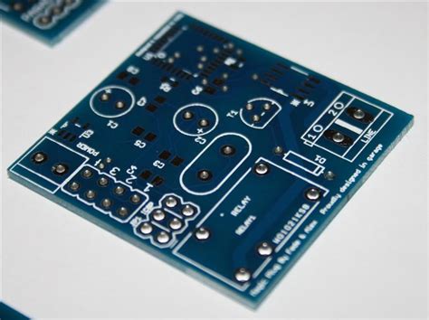
What is a PCB?
A printed circuit board (PCB) is a fundamental component in modern electronics. It is a thin board made of insulating materials, such as fiberglass or composite epoxy, with conductive copper traces etched onto its surface. These traces connect various electronic components, such as resistors, capacitors, and integrated circuits, to form a complete electronic circuit.
PCBs offer several advantages over traditional point-to-point wiring:
- Compact and organized layout
- Improved reliability and durability
- Easier troubleshooting and repair
- Increased efficiency in mass production
Why Make Your Own PCBs?
Creating your own PCBs at home offers several benefits:
- Cost-effective: Making your own PCBs can be more affordable than ordering them from a manufacturer, especially for small-scale projects or prototypes.
- Customization: You have complete control over the design and layout of your PCB, allowing you to tailor it to your specific needs.
- Learning experience: Designing and fabricating your own PCBs is an excellent way to learn about electronics and develop your skills.
- Faster turnaround: By making your own PCBs, you can avoid the waiting time associated with ordering from a manufacturer, allowing you to iterate and test your designs more quickly.

Tools and Materials Required
To get started with making your own PCBs at home, you’ll need the following tools and materials:
- Copper-clad board
- PCB design software (e.g., KiCad, Eagle)
- Laser printer or photoplotter
- Transparency film
- UV exposure unit or sunlight
- Developer solution (e.g., sodium hydroxide)
- Etching solution (e.g., ferric chloride)
- Drill or drill press
- Safety equipment (gloves, goggles, etc.)
| Tool/Material | Purpose |
|---|---|
| Copper-clad board | The base material for your PCB |
| PCB design software | For designing the PCB layout |
| Laser printer or photoplotter | To print the PCB design onto transparency film |
| Transparency film | For creating the photomask |
| UV exposure unit or sunlight | To expose the photoresist on the copper-clad board |
| Developer solution | To develop the exposed photoresist |
| Etching solution | To remove the unwanted copper from the board |
| Drill or drill press | For drilling holes in the PCB |
| Safety equipment | To protect yourself during the PCB fabrication process |

Step-by-Step Guide to Making PCBs at Home
Step 1: Design Your PCB
The first step in making your own PCB is to design the circuit using PCB design software. There are several free and paid options available, such as KiCad and Eagle. These software packages allow you to create schematic diagrams, design the PCB layout, and generate the necessary files for fabrication.
When designing your PCB, keep the following considerations in mind:
- Component placement and orientation
- Trace width and spacing
- Ground planes and power distribution
- Mounting holes and mechanical constraints
Step 2: Create the Photomask
Once you have completed your PCB design, you need to create a photomask that will be used to transfer the design onto the copper-clad board. To create the photomask, print the PCB layout onto a transparency film using a laser printer or photoplotter. Make sure the printed design is dark and opaque, as this will ensure a clean transfer to the copper-clad board.
Step 3: Prepare the Copper-Clad Board
Clean the copper-clad board thoroughly with steel wool or fine sandpaper to remove any oxidation or contaminants. This will help ensure proper adhesion of the photoresist and improve the quality of the final PCB.
Step 4: Apply Photoresist
Apply a thin, even layer of photoresist to the copper-clad board. You can use pre-sensitized boards or apply the photoresist manually using a spray or roller. Follow the manufacturer’s instructions for the specific photoresist you are using.
Step 5: Expose the PCB
Place the photomask on top of the photoresist-coated copper-clad board and expose it to UV light. You can use a UV exposure unit or sunlight for this step. The exposure time will depend on the type of photoresist and the intensity of the UV light source. Consult the manufacturer’s guidelines for the recommended exposure time.
Step 6: Develop the PCB
After exposure, immerse the PCB in a developer solution to remove the unexposed photoresist. The developer solution will typically be a weak alkaline solution, such as sodium hydroxide. Agitate the board gently until the unexposed photoresist has been completely removed, revealing the copper traces underneath.
Step 7: Etch the PCB
Once the PCB has been developed, it’s time to etch away the unwanted copper. Immerse the board in an etching solution, such as ferric chloride, and agitate it gently. The etching process will remove the copper that is not protected by the developed photoresist, leaving behind the desired copper traces. Monitor the etching process closely and remove the board once all the unwanted copper has been removed.
Step 8: Clean and Drill the PCB
After etching, rinse the PCB thoroughly with water and remove the remaining photoresist using a solvent or by gently scrubbing with steel wool. Inspect the board for any defects or incomplete etching, and touch up as necessary.
Finally, drill any required holes for component leads or mounting using a drill or drill press. Be sure to use the appropriate drill bit size for your components.

Tips and Tricks for Successful PCB Fabrication
- Double-check your design: Before proceeding with fabrication, thoroughly review your PCB design for any errors or potential issues. Catching mistakes early can save you time and resources.
- Maintain a clean workspace: Keep your work area clean and organized to prevent contamination of your PCB during the fabrication process.
- Use high-quality materials: Invest in high-quality copper-clad boards, photoresist, and chemicals to ensure the best possible results.
- Practice proper safety: Always wear appropriate safety equipment, such as gloves and goggles, when handling chemicals and working with power tools.
- Experiment and iterate: Don’t be discouraged if your first attempts at PCB fabrication are not perfect. Keep experimenting, learning, and refining your techniques to improve your results over time.
Frequently Asked Questions (FAQ)
-
Can I make double-sided PCBs at home?
Yes, it is possible to make double-sided PCBs at home using a similar process. However, you will need to ensure proper alignment of the designs on both sides of the board and use through-hole plating techniques to connect the layers. -
What is the best PCB design software for beginners?
Some popular PCB design software options for beginners include KiCad, Eagle, and EasyEDA. These software packages offer user-friendly interfaces, extensive component libraries, and comprehensive tutorials to help you get started. -
How can I improve the resolution of my PCB traces?
To improve the resolution of your PCB traces, use a high-quality laser printer or photoplotter to create your photomask. Ensure that the printed design is dark and opaque, and experiment with different exposure times to find the optimal settings for your setup. -
What should I do if my PCB has incomplete etching or short circuits?
If your PCB has incomplete etching or short circuits, you can try touching up the affected areas with a permanent marker or etch-resistant paint and re-etching the board. For more severe issues, you may need to start over with a new copper-clad board and review your design and fabrication process for potential improvements. -
Can I use the same etching solution multiple times?
Yes, you can reuse etching solutions such as ferric chloride multiple times. However, the etching process will become slower as the solution becomes saturated with copper. To extend the life of your etching solution, you can regenerate it using methods such as aeration or electrolysis.
Conclusion
Making your own PCBs at home is a rewarding and educational experience that can help you bring your electronic projects to life. By following the steps outlined in this article and practicing proper safety and technique, you can create high-quality PCBs for your projects. Remember to start with simple designs, be patient, and learn from your mistakes as you refine your skills. With time and practice, you’ll be able to create increasingly complex and professional-looking PCBs in the comfort of your own home.


Leave a Reply