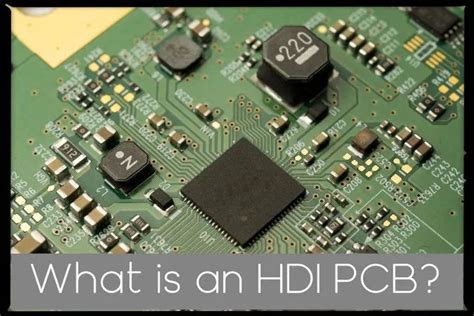
What is HDI PCB?
HDI PCB, which stands for High Density Interconnector Printed Circuit Board, is a type of PCB that has a higher wiring density per unit area than conventional PCBs. This is achieved by utilizing smaller vias, finer trace widths and spaces, and advanced fabrication techniques. HDI PCBs are designed to meet the demands of miniaturization, high performance, and increased functionality in modern electronic devices.
The main characteristics of HDI PCBs include:
- Smaller vias (microvias) with diameters less than 150 μm
- Finer trace widths and spaces, typically less than 100 μm
- Higher layer counts (usually 8 or more)
- Buried and blind vias for increased routing density
- Sequential lamination process for fabrication
HDI PCBs find applications in various industries, such as:
- Consumer electronics (smartphones, tablets, wearables)
- Automotive (infotainment systems, ADAS)
- Medical devices (implantable devices, diagnostic equipment)
- Aerospace and defense (avionics, radar systems)
- Telecommunications (5G devices, network equipment)
Advantages of HDI PCBs
Miniaturization
One of the primary advantages of HDI PCBs is their ability to enable miniaturization of electronic devices. By utilizing smaller vias and finer traces, designers can pack more functionality into a smaller footprint. This is particularly important for devices like smartphones, smartwatches, and other wearables where space is at a premium.
Improved Signal Integrity
HDI PCBs offer improved signal integrity compared to traditional PCBs. The shorter signal paths and reduced layer count result in lower signal loss, crosstalk, and electromagnetic interference (EMI). This is crucial for high-speed applications, such as 5G devices and high-performance computing systems.
Increased Reliability
The use of microvias and advanced fabrication techniques in HDI PCBs contributes to increased reliability. Microvias have a smaller aspect ratio (depth to diameter ratio) compared to through-hole vias, which reduces the risk of via failures due to thermal stress or mechanical strain. Additionally, the sequential lamination process used in HDI PCB Fabrication ensures better interlayer bonding and reduces the likelihood of delamination.
Cost-Effective
Although HDI PCBs have a higher cost per unit area compared to traditional PCBs, they can be cost-effective in the long run. The increased functionality and miniaturization enabled by HDI technology can lead to reduced overall system costs, as fewer components and less packaging are required. Furthermore, the improved reliability of HDI PCBs can result in lower maintenance and repair costs over the product lifecycle.

HDI PCB Design Considerations
Layer Stack-up
Designing an efficient layer stack-up is crucial for achieving a perfect HDI PCB. The layer stack-up should be optimized to minimize signal loss, crosstalk, and EMI while ensuring manufacturability. Some key considerations include:
- Use of high-performance laminate materials with low dielectric constants and Loss Tangents
- Proper placement of power and ground planes to provide shielding and reduce EMI
- Minimizing the number of layer transitions for critical signals
- Utilization of blind and buried vias for increased routing density
Here’s an example of a typical 8-layer HDI PCB Stack-up:
| Layer | Type | Material | Thickness (μm) |
|---|---|---|---|
| 1 | Signal | Copper | 18 |
| 2 | Ground | Copper | 35 |
| 3 | Signal | Copper | 18 |
| 4 | Signal | Copper | 18 |
| 5 | Power | Copper | 35 |
| 6 | Signal | Copper | 18 |
| 7 | Signal | Copper | 18 |
| 8 | Signal | Copper | 18 |
Via Types and Placement
HDI PCBs utilize various types of vias, including through-hole, blind, and buried vias. Selecting the appropriate via type and optimizing their placement is essential for achieving a perfect HDI design.
- Through-hole vias: These vias extend through all layers of the PCB and are used for connecting components to the board or for layer transitions.
- Blind vias: These vias connect an outer layer to an inner layer, but do not extend through the entire board thickness. Blind vias are used for increased routing density and to minimize layer transitions.
- Buried vias: These vias connect two or more inner layers without extending to the outer layers. Buried vias are used for even higher routing density and to reduce the number of layer transitions.
When placing vias, designers should consider the following:
- Minimize the use of through-hole vias in high-density areas
- Place vias as close to the components as possible to reduce signal path length
- Avoid placing vias in critical signal paths to minimize signal integrity issues
- Use via-in-pad design when possible to further increase routing density
Trace Width and Spacing
HDI PCBs feature finer trace widths and spaces compared to traditional PCBs. The specific trace width and spacing requirements depend on the application, the manufacturing capabilities of the PCB fabricator, and the design rules provided by the component manufacturers.
Typical trace width and spacing for HDI PCBs range from 75 μm to 100 μm. However, some advanced HDI designs may utilize trace widths and spaces as small as 50 μm.
When designing traces for HDI PCBs, consider the following:
- Use appropriate trace widths based on the required current carrying capacity and signal integrity requirements
- Maintain consistent trace impedance throughout the signal path to minimize reflections and signal distortion
- Follow the manufacturer’s recommended design rules for trace width and spacing
- Use serpentine routing techniques to match trace lengths for differential pairs and critical signals

HDI PCB Fabrication Process
The fabrication process for HDI PCBs is more complex than that of traditional PCBs due to the smaller features and advanced techniques involved. The key steps in HDI PCB fabrication include:
- Inner layer processing: The inner layers of the PCB are fabricated using standard PCB manufacturing techniques, such as etching and drilling.
- Sequential lamination: The inner layers are laminated together in a sequential manner, with microvias drilled and filled between each lamination step.
- Outer layer processing: The outer layers of the PCB are fabricated and laminated to the inner layer stack.
- Drilling and plating: Through-hole vias are drilled and plated, and any remaining microvias are filled and plated.
- Solder mask and surface finish: The PCB is coated with a solder mask and a surface finish, such as ENIG (Electroless Nickel Immersion Gold) or OSP (Organic Solderability Preservative), is applied.

Testing and Quality Control
To ensure the perfect functioning of an HDI PCB, rigorous testing and quality control measures must be implemented throughout the fabrication process. Some essential testing and quality control steps include:
- Visual inspection: The PCB is visually inspected for any surface defects, such as scratches, dents, or discoloration.
- Automated Optical Inspection (AOI): An automated optical inspection system is used to detect any manufacturing defects, such as short circuits, open circuits, or incorrect component placement.
- Electrical testing: The PCB undergoes various electrical tests, such as continuity testing, insulation resistance testing, and high-potential (HiPot) testing, to ensure proper electrical functioning.
- Microsectioning: A small section of the PCB is cut and analyzed under a microscope to verify the integrity of the vias, traces, and lamination.
- Thermal cycling: The PCB is subjected to multiple thermal cycles to ensure its ability to withstand temperature fluctuations during operation.
By implementing these testing and quality control measures, manufacturers can ensure that the HDI PCBs meet the required specifications and perform reliably in their intended applications.
Frequently Asked Questions (FAQ)
1. What is the minimum via size achievable in HDI PCBs?
The minimum via size in HDI PCBs depends on the fabrication capabilities of the PCB manufacturer. Typically, microvias in HDI PCBs can have diameters ranging from 75 μm to 150 μm. However, some advanced HDI PCB fabrication processes can achieve via diameters as small as 50 μm.
2. How many layers can an HDI PCB have?
HDI PCBs can have a varying number of layers, depending on the complexity and requirements of the application. Most HDI PCBs have 8 or more layers, with some designs extending up to 24 layers or more. The number of layers is determined by factors such as signal routing density, power distribution, and overall board thickness constraints.
3. What are the common materials used in HDI PCB fabrication?
HDI PCBs typically use high-performance laminate materials with low dielectric constants (Dk) and low loss tangents (Df) to minimize signal loss and improve signal integrity. Some common materials used in HDI PCB fabrication include:
- FR-4: A glass-reinforced epoxy laminate, which is the most widely used material in PCB fabrication.
- Isola 370HR: A high-performance laminate with a low Dk and Df, suitable for high-speed applications.
- Rogers 4350B: A hydrocarbon ceramic laminate with excellent thermal stability and low loss properties, ideal for RF and microwave applications.
4. How does the cost of HDI PCBs compare to traditional PCBs?
HDI PCBs generally have a higher cost per unit area compared to traditional PCBs due to the advanced fabrication techniques and materials used. However, the overall system cost can be lower with HDI PCBs, as they enable miniaturization and increased functionality, reducing the number of components and packaging requirements. The cost-effectiveness of HDI PCBs depends on the specific application and production volume.
5. What are the key challenges in HDI PCB design and fabrication?
Some of the key challenges in HDI PCB design and fabrication include:
-
Signal integrity: Maintaining signal integrity becomes more challenging with the smaller features and higher routing density of HDI PCBs. Designers must carefully consider factors such as trace impedance, signal path length, and via placement to minimize signal distortion and crosstalk.
-
Thermal management: The increased component density and higher power dissipation in HDI PCBs can lead to thermal management challenges. Designers must incorporate appropriate thermal management techniques, such as the use of thermal vias, heatsinks, and proper component placement, to ensure reliable operation.
-
Manufacturing complexity: The smaller features and advanced fabrication techniques used in HDI PCBs require stricter process control and higher precision equipment. This increased complexity can lead to higher manufacturing costs and longer lead times compared to traditional PCBs.
-
Design for manufacturability (DFM): Designing HDI PCBs that are manufacturable and meet the required specifications can be challenging. Designers must work closely with PCB Fabricators to ensure that the design adheres to the manufacturer’s capabilities and design rules, minimizing the risk of fabrication issues and delays.
Conclusion
HDI PCBs offer numerous advantages over traditional PCBs, including miniaturization, improved signal integrity, increased reliability, and cost-effectiveness in the long run. However, achieving a perfect HDI PCB design and fabrication requires careful consideration of various factors, such as layer stack-up, via types and placement, trace width and spacing, and material selection.
By following best practices in HDI PCB design, working closely with experienced PCB fabricators, and implementing rigorous testing and quality control measures, designers and manufacturers can create perfect HDI PCBs that meet the demands of today’s advanced electronic devices.
As technology continues to evolve, the importance of HDI PCBs will only grow, driving innovation and enabling the development of smaller, faster, and more powerful electronic devices across various industries.


Leave a Reply