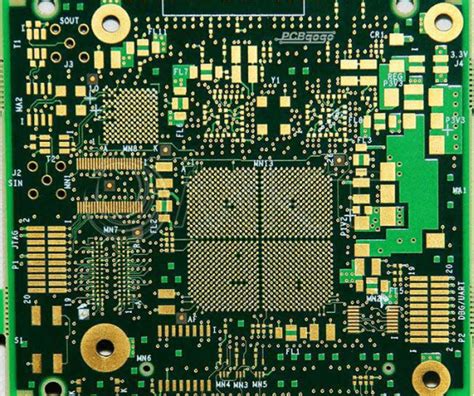
What is HDI PCB Design?
HDI PCB design is a type of printed circuit board design that incorporates high-density interconnects, allowing for a greater number of components to be placed on a smaller board area. This is achieved through the use of smaller vias, finer trace widths, and multiple layers.
The main characteristics of HDI PCBs include:
– Via diameters less than 6 mils (0.15mm)
– Line widths and spacings less than 4 mils (0.1mm)
– Capture pad diameters less than 12 mils (0.3mm)
– Higher layer counts (8 or more)
Advantages of HDI PCB Design
-
Miniaturization: HDI PCBs enable the creation of smaller, more compact devices, which is crucial in industries such as consumer electronics, wearables, and medical devices.
-
Improved Signal Integrity: The shorter signal paths and reduced layer count in HDI PCBs lead to improved signal integrity, minimizing issues like crosstalk and electromagnetic interference (EMI).
-
Enhanced Thermal Management: HDI PCBs offer better thermal management due to the increased surface area for heat dissipation and the ability to place thermal vias near heat-generating components.
-
Cost-Effective: Although the initial cost of HDI PCBs may be higher than traditional PCBs, they often result in cost savings in the long run due to reduced assembly time, fewer manufacturing defects, and improved reliability.
HDI PCB design guidelines
To create a successful HDI PCB design, consider the following guidelines:
1. Choose the Right PCB Material
The choice of PCB material is crucial in HDI design. The most common materials used are:
- FR-4: A standard, cost-effective material suitable for most applications.
- High-Tg FR-4: Offers better thermal stability and is suitable for lead-free soldering processes.
- Polyimide: Provides excellent thermal stability and is ideal for high-temperature applications.
- Rogers: Offers superior high-frequency performance and is suitable for RF and microwave applications.
2. Optimize Component Placement
Proper component placement is essential for HDI PCB design. Follow these tips:
- Place components on both sides of the board to maximize space utilization.
- Group related components together to minimize signal path lengths.
- Consider the height of components and ensure adequate clearance for assembly.
- Place heat-generating components near the board edges or thermal vias for better heat dissipation.
3. Use Blind and Buried Vias
Blind and buried vias are essential in HDI PCB design as they allow for more efficient use of board space and improved signal routing. Blind vias connect an outer layer to an inner layer, while buried vias connect two or more inner layers without reaching the outer layers.
When using blind and buried vias, keep in mind:
– The aspect ratio (depth to diameter) should be less than 1:1 for reliable plating.
– The via size should be as small as possible while still ensuring manufacturability.
– Stagger vias to avoid creating a weak spot in the board.
4. Minimize Via Stubs
Via stubs are the unused portion of a via that extends beyond the target layer. In high-speed designs, via stubs can cause signal reflections and degrade signal integrity. To minimize via stubs:
- Use back-drilling to remove the unused portion of the via.
- Employ blind and buried vias to reduce the overall via length.
- Consider using microvias, which have a smaller diameter and shorter stub length.
5. Implement Differential Pair Routing
Differential signaling is commonly used in high-speed digital interfaces like USB, HDMI, and PCIe. When routing differential pairs in HDI PCBs:
- Keep the trace lengths matched within 5 mils (0.13mm) to maintain signal integrity.
- Maintain a consistent spacing between the traces to ensure a stable differential impedance.
- Avoid sharp bends and use smooth curves to minimize signal reflections.
6. Utilize High-Density BGA Packaging
Ball Grid Array (BGA) packages are ideal for HDI PCB design due to their high pin count and small footprint. When using BGAs:
- Choose a ball pitch that is compatible with your PCB fabrication capabilities.
- Use a via-in-pad design to maximize routing space and minimize signal path lengths.
- Ensure adequate solder mask clearance around the BGA pads to prevent shorts during assembly.

HDI PCB Stackup Design
The stackup is a critical aspect of HDI PCB design, as it determines the number of layers, their arrangement, and the interconnections between them. A well-designed stackup ensures signal integrity, manufacturability, and reliability.
HDI PCB Stackup Examples
Here are some common HDI PCB Stackups:
- 4-Layer Stackup
- Layer 1: Signal
- Layer 2: Ground
- Layer 3: Power
-
Layer 4: Signal
-
6-Layer Stackup
- Layer 1: Signal
- Layer 2: Ground
- Layer 3: Signal
- Layer 4: Signal
- Layer 5: Power
-
Layer 6: Signal
-
8-Layer Stackup
- Layer 1: Signal
- Layer 2: Ground
- Layer 3: Signal
- Layer 4: Power
- Layer 5: Signal
- Layer 6: Ground
- Layer 7: Signal
- Layer 8: Signal
HDI PCB Stackup Design Considerations
When designing your HDI PCB stackup, consider the following:
- Use a symmetrical stackup to minimize warpage and ensure even copper distribution.
- Alternate signal and plane layers to provide a consistent reference plane for signal traces.
- Use a minimum of two ground layers for better shielding and EMI reduction.
- Place power layers close to the components they serve to minimize voltage drop and noise.
- Use thin dielectric materials to reduce overall board thickness and improve signal performance.

HDI PCB Manufacturing Process
The manufacturing process for HDI PCBs is more complex than traditional PCBs due to the smaller features and higher layer counts. The main steps involved are:
-
Material Selection: Choose the appropriate PCB material based on your design requirements.
-
Drilling: Drill the vias using laser or mechanical drilling methods. Laser drilling is preferred for HDI PCBs due to its ability to create smaller, more precise vias.
-
Plating: Plate the vias and traces with copper to establish electrical connections between layers. This step may involve multiple plating cycles for blind and buried vias.
-
Patterning: Create the circuit patterns on each layer using photolithography and etching processes.
-
Lamination: Laminate the layers together using heat and pressure to form the complete PCB stackup.
-
Surface Finish: Apply the desired surface finish (e.g., ENIG, HASL, or OSP) to protect the exposed copper and facilitate component assembly.
-
Electrical Testing: Perform electrical tests to ensure the PCB meets the required specifications and functionality.

HDI PCB Design Software
To create HDI PCB designs, you’ll need to use specialized PCB design software. Some popular options include:
-
Altium Designer: A comprehensive PCB design package with advanced features for HDI design, including 3D modeling and simulation.
-
Cadence Allegro: A powerful PCB design solution with support for high-speed design, constraint management, and HDI capabilities.
-
Mentor Graphics PADS: A scalable PCB design platform with tools for HDI design, signal integrity analysis, and thermal management.
-
OrCAD PCB Designer: A user-friendly PCB design software with support for HDI design, constraint-driven layout, and simulation.
FAQ
1. What is the minimum via size for HDI PCBs?
The minimum via size for HDI PCBs is typically 6 mils (0.15mm) in diameter. However, this can vary depending on the PCB fabricator’s capabilities and the specific design requirements.
2. How many layers are typically used in HDI PCBs?
HDI PCBs typically have 8 or more layers, although 4-layer and 6-layer designs are also common. The number of layers depends on the complexity of the design and the required functionality.
3. What is the difference between blind and buried vias?
Blind vias connect an outer layer to an inner layer, while buried vias connect two or more inner layers without reaching the outer layers. Both types of vias are essential in HDI PCB design for efficient space utilization and improved signal routing.
4. Can HDI PCBs be used for high-power applications?
Yes, HDI PCBs can be used for high-power applications with proper thermal management techniques, such as using thicker copper layers, incorporating thermal vias, and selecting appropriate PCB materials with good thermal conductivity.
5. Are HDI PCBs more expensive than traditional PCBs?
The initial cost of HDI PCBs is typically higher than traditional PCBs due to the more complex manufacturing process and the use of advanced materials. However, HDI PCBs often result in cost savings in the long run due to reduced assembly time, fewer manufacturing defects, and improved reliability.
Conclusion
HDI PCB design is a powerful tool for creating smaller, more complex electronic devices with improved signal integrity and thermal management. By following the guidelines and best practices outlined in this article, you can create the most suitable HDI PCB design for your needs. Remember to choose the right PCB material, optimize component placement, use blind and buried vias, minimize via stubs, implement differential pair routing, and utilize high-density BGA packaging. With the right design software and a well-planned stackup, you can unlock the full potential of HDI PCBs and bring your electronic products to the next level.


Leave a Reply