Introduction to PCB Design and KiCad
Printed Circuit Boards (PCBs) are the backbone of modern electronics. They provide a stable and efficient way to connect electronic components and create complex circuits. Designing a PCB can be a daunting task, especially for beginners. However, with the right tools and guidance, anyone can create a professional-grade PCB. In this guide, we will focus on using KiCad, a free and open-source software suite for electronic design automation (EDA), to create a PCB from scratch.
What is KiCad?
KiCad is a cross-platform software suite that provides a complete set of tools for electronic design, including schematic capture, PCB layout, and 3D visualization. It is widely used by hobbyists, students, and professionals alike for its user-friendly interface, extensive libraries, and powerful features. KiCad is continuously updated and maintained by a community of developers and users, ensuring its stability and reliability.
Why Choose KiCad for PCB Design?
There are several reasons why KiCad is an excellent choice for PCB design:
- Free and Open-Source: KiCad is completely free to use and distribute, making it accessible to everyone regardless of budget constraints.
- Cross-Platform Compatibility: KiCad runs on Windows, macOS, and Linux, allowing users to work on their preferred operating system.
- User-Friendly Interface: KiCad has a well-designed and intuitive user interface that makes it easy for beginners to get started while providing advanced features for experienced users.
- Extensive Libraries: KiCad comes with a large collection of component libraries, and users can easily create their own or import third-party libraries.
- Active Community: KiCad has a vibrant and supportive community of users and developers who provide tutorials, forums, and resources to help users learn and troubleshoot.
Getting Started with KiCad
Before diving into the PCB design process, it is essential to set up KiCad and familiarize yourself with its interface and tools.
Installing KiCad
To install KiCad, follow these steps:
- Visit the official KiCad website: https://www.kicad.org/
- Click on the “Download” button and select your operating system.
- Download the appropriate installer for your system.
- Run the installer and follow the on-screen instructions.
KiCad’s Main Components
KiCad consists of several main components that work together to create a complete PCB design:
- Eeschema: The schematic editor for creating circuit diagrams.
- Pcbnew: The PCB layout editor for designing the physical board.
- Cvpcb: The footprint association tool for assigning component footprints.
- GerbView: The Gerber viewer for inspecting and verifying Gerber files.
- Bitmap2Component: A tool for converting images into component footprints.
KiCad Workflow
The typical KiCad workflow involves the following steps:
- Create a schematic in Eeschema.
- Assign footprints to components using Cvpcb.
- Layout the PCB in Pcbnew.
- Generate Gerber files for manufacturing.
- Inspect and verify Gerber files using GerbView.

Designing a Schematic in Eeschema
The first step in creating a PCB is to design the schematic, which represents the electrical connections between components. Eeschema is KiCad’s schematic editor that allows you to create, edit, and manage circuit diagrams.
Creating a New Schematic
To create a new schematic in Eeschema, follow these steps:
- Open KiCad and click on the “Eeschema” button.
- Click on “File” > “New” to create a new schematic.
- Save the schematic file with a descriptive name.
Adding Components
To add components to your schematic, follow these steps:
- Click on the “Place Symbol” button in the toolbar or press the “A” key.
- Search for the desired component in the library browser.
- Click on the component to select it and then click on the schematic to place it.
- Repeat the process for all the required components.
Connecting Components
To connect components in your schematic, follow these steps:
- Click on the “Place Wire” button in the toolbar or press the “W” key.
- Click on the starting point of the connection (e.g., a component pin).
- Click on the endpoint of the connection (e.g., another component pin).
- Repeat the process for all the required connections.
Annotating and Labeling
To annotate and label your schematic, follow these steps:
- Click on the “Annotate Schematic” button in the toolbar or press the “T” key.
- Select the annotation options and click “Annotate.”
- Click on the “Place Net Label” button in the toolbar or press the “L” key.
- Click on a wire and enter the net label.
- Repeat the process for all the required net labels.

Assigning Footprints with Cvpcb
Once the schematic is complete, the next step is to assign footprints to the components. Footprints define the physical dimensions and layout of the components on the PCB. Cvpcb is the footprint association tool in KiCad that allows you to assign footprints to components.
Generating a Netlist
To generate a netlist for Cvpcb, follow these steps:
- In Eeschema, click on “Tools” > “Generate Netlist.”
- Select the output format as “Pcbnew” and click “Generate.”
- Save the netlist file.
Assigning Footprints
To assign footprints to components using Cvpcb, follow these steps:
- Open Cvpcb from the KiCad main window.
- Load the netlist file generated in the previous step.
- For each component, double-click on the footprint column and select the appropriate footprint from the library.
- Save the footprint association file.

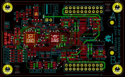
Laying Out the PCB in Pcbnew
With the schematic and footprint association complete, the next step is to layout the PCB in Pcbnew. Pcbnew is the PCB layout editor in KiCad that allows you to design the physical board, place components, route traces, and add various design elements.
Creating a New PCB Layout
To create a new PCB layout in Pcbnew, follow these steps:
- Open Pcbnew from the KiCad main window.
- Click on “File” > “New” to create a new PCB layout.
- Save the PCB layout file with a descriptive name.
Setting Up the Board
To set up the board properties and dimensions, follow these steps:
- Click on “File” > “Board Setup.”
- Set the board dimensions, grid size, and other properties as required.
- Click “OK” to apply the changes.
Importing the Netlist
To import the netlist generated from Eeschema, follow these steps:
- Click on “Tools” > “Update PCB from Schematic.”
- Select the netlist file and click “Open.”
- Review the changes and click “Update PCB.”
Placing Components
To place components on the PCB, follow these steps:
- Click on the “Place Footprints” button in the toolbar or press the “O” key.
- Select the component to place and click on the desired location on the PCB.
- Repeat the process for all the components.
Routing Traces
To route traces between components, follow these steps:
- Click on the “Route Tracks” button in the toolbar or press the “X” key.
- Select the appropriate track width and layer.
- Click on the starting pad and then click on the ending pad to route the trace.
- Repeat the process for all the required connections.
Adding Design Elements
To add design elements such as silkscreen, solder mask, and text, follow these steps:
- Click on the appropriate button in the toolbar (e.g., “Add Graphic Line,” “Add Graphic Polygon,” “Add Text”).
- Select the desired layer and properties.
- Place the design element on the PCB.
Generating Gerber Files
Once the PCB layout is complete, the next step is to generate Gerber files for manufacturing. Gerber files are industry-standard files that contain the necessary information for PCB fabrication.
Configuring Plot Settings
To configure the plot settings for generating Gerber files, follow these steps:
- In Pcbnew, click on “File” > “Plot.”
- Select the appropriate layers to plot (e.g., copper layers, silkscreen, solder mask).
- Set the plot format to “Gerber.”
- Choose the output directory and click “Plot.”
Generating Drill Files
To generate drill files for the PCB, follow these steps:
- In Pcbnew, click on “File” > “Generate Drill Files.”
- Select the appropriate drill file format (e.g., Excellon).
- Choose the output directory and click “Generate.”
Inspecting and Verifying Gerber Files
Before sending the Gerber files to a PCB manufacturer, it is essential to inspect and verify them to ensure accuracy and avoid costly mistakes. GerbView is the Gerber viewer in KiCad that allows you to inspect and verify Gerber files.
Loading Gerber Files
To load Gerber files in GerbView, follow these steps:
- Open GerbView from the KiCad main window.
- Click on “File” > “Load Layers.”
- Select the Gerber files generated in the previous step and click “Open.”
Inspecting Gerber Files
To inspect the Gerber files, follow these steps:
- Use the zoom and pan tools to navigate around the PCB.
- Check for any obvious errors or discrepancies.
- Verify that all the layers align correctly.
Verifying Gerber Files
To verify the Gerber files, follow these steps:
- Click on “File” > “Compare Layers.”
- Select the layers to compare and click “Compare.”
- Review the comparison results and address any issues found.
FAQ
-
Can I use KiCad for commercial projects?
Yes, KiCad is free and open-source software, and you can use it for both personal and commercial projects without any restrictions. -
Is KiCad suitable for beginners?
Yes, KiCad has a user-friendly interface and extensive documentation, making it suitable for beginners. However, it is recommended to have a basic understanding of electronics and PCB design concepts before starting. -
Can I import designs from other EDA software into KiCad?
Yes, KiCad supports importing designs from various formats, including Eagle, Altium, and OrCAD. However, some manual adjustments may be required to ensure compatibility. -
How can I share my KiCad projects with others?
You can share your KiCad projects by packaging all the necessary files (schematic, PCB layout, libraries) into a single archive (e.g., ZIP file) and sharing it with others. They can then import the project into their KiCad installation. -
Where can I find additional resources and support for KiCad?
The official KiCad website (https://www.kicad.org/) provides a wealth of resources, including documentation, tutorials, and a forum where you can ask questions and get support from the KiCad community. Additionally, there are numerous third-party websites, blogs, and YouTube channels dedicated to KiCad tutorials and projects.
Conclusion
Creating a PCB with KiCad is a straightforward process that can be mastered with practice and patience. By following this guide, you should have a solid understanding of the KiCad workflow, from designing the schematic to generating Gerber files for manufacturing. Remember to take advantage of the extensive libraries, user-friendly interface, and supportive community that KiCad offers. With KiCad, you have the power to bring your electronic designs to life and create professional-grade PCBs.


Leave a Reply