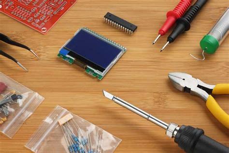
Introduction to PCB Tools
Printed Circuit Board (PCB) design and manufacturing is a complex process that requires specialized tools for programming and testing. These tools are essential for ensuring the quality, reliability, and functionality of PCBs. In this article, we will explore 11 key aspects of PCB programming and testing tools that every engineer and technician should know.
1. PCB Design Software
1.1 Types of PCB Design Software
There are various types of PCB design software available in the market, including:
– Schematic Capture Software
– PCB Layout Software
– Circuit Simulation Software
– 3D Modeling Software
1.2 Popular PCB Design Software
Some of the popular PCB design software used in the industry are:
– Altium Designer
– KiCad
– Eagle
– OrCAD
– Cadence Allegro
1.3 Choosing the Right PCB Design Software
When selecting PCB design software, consider the following factors:
– Ease of use and learning curve
– Features and capabilities
– Compatibility with other tools and formats
– Cost and licensing options
– Community support and resources

2. PCB Programming Tools
2.1 In-System Programming (ISP)
In-System Programming (ISP) is a method of programming a device while it is installed in the target system. ISP tools allow you to program microcontrollers, EEPROMs, and other programmable devices directly on the PCB.
2.2 JTAG Programming
JTAG (Joint Test Action Group) is a standard interface for debugging and programming devices on a PCB. JTAG programming tools enable you to access and control the internal registers and memory of a device for testing and debugging purposes.
2.3 Boundary Scan Testing
Boundary Scan Testing is a method of testing the interconnections between devices on a PCB without the need for physical access to the pins. It uses a special boundary scan cell in each device to control and observe the pin states.

3. PCB Testing Tools
3.1 In-Circuit Testing (ICT)
In-Circuit Testing (ICT) is a method of testing the functionality of individual components on a PCB by directly accessing their pins. ICT tools use a bed-of-nails fixture to make contact with the component pins and perform various tests.
3.2 Flying Probe Testing
Flying Probe Testing is a non-contact testing method that uses movable probes to test the connections and components on a PCB. It is more flexible than ICT but slower in terms of testing speed.
3.3 Automated Optical Inspection (AOI)
Automated Optical Inspection (AOI) is a visual inspection method that uses cameras and image processing algorithms to detect defects and anomalies on a PCB. AOI tools can identify issues such as missing components, solder defects, and incorrect component placement.

4. PCB Functional Testing
4.1 Functional Test Fixtures
Functional test fixtures are specialized jigs or enclosures that hold the PCB and provide the necessary connections and stimuli for functional testing. They are designed to simulate the actual operating conditions of the PCB.
4.2 Functional Test Software
Functional test software is used to create and execute test programs for verifying the functionality of a PCB. It typically includes features such as test sequencing, data logging, and report generation.
4.3 Boundary Scan Functional Testing
Boundary Scan Functional Testing combines boundary scan technology with functional testing to verify the functionality of a PCB at the board level. It allows testing of the interconnections and the internal logic of the devices on the PCB.
5. PCB Debugging Tools
5.1 Logic Analyzers
Logic analyzers are tools used for capturing and analyzing digital signals on a PCB. They help in troubleshooting and debugging digital circuits by displaying the timing relationships and states of multiple signals simultaneously.
5.2 Oscilloscopes
Oscilloscopes are instruments used for visualizing and measuring analog signals on a PCB. They display the waveform of the signal over time and allow measurement of parameters such as voltage, frequency, and rise/fall times.
5.3 Thermal Imaging Cameras
Thermal imaging cameras are used for detecting hot spots and thermal issues on a PCB. They provide a visual representation of the temperature distribution on the board, helping in identifying components that are overheating or thermal management problems.
6. PCB Rework and Repair Tools
6.1 Soldering Irons and Stations
Soldering irons and stations are essential tools for PCB rework and repair. They are used for soldering and desoldering components, making modifications, and fixing defects on the PCB.
6.2 Desoldering Tools
Desoldering tools, such as desoldering pumps and desoldering wicks, are used for removing solder and components from a PCB. They are necessary for replacing faulty components or making modifications to the board.
6.3 Rework Stations
Rework stations are advanced tools that combine soldering, desoldering, and hot air functions in a single unit. They provide precise control over temperature and airflow, making them suitable for complex rework tasks.
7. PCB Inspection Tools
7.1 Microscopes
Microscopes are used for visual inspection of PCBs at high magnification. They help in identifying defects, such as solder bridges, damaged traces, or component issues, that may not be visible to the naked eye.
7.2 X-Ray Inspection Systems
X-Ray inspection systems are used for non-destructive testing of PCBs. They provide a detailed internal view of the board, allowing detection of hidden defects, such as voids in solder joints or component alignment issues.
7.3 3D Automated Inspection Systems
3D automated inspection systems use multiple cameras and advanced algorithms to create a three-dimensional model of the PCB. They can detect defects related to component height, coplanarity, and solder joint quality.
8. PCB Manufacturing Tools
8.1 PCB Prototyping Machines
PCB prototyping machines, such as desktop CNC mills and 3D printers, allow rapid prototyping of PCBs in-house. They are useful for creating quick iterations and testing designs before mass production.
8.2 Pick-and-Place Machines
Pick-and-Place machines are used for automatically placing components on a PCB during the assembly process. They ensure precise and efficient placement of components, reducing the chances of human error.
8.3 Reflow Ovens
Reflow ovens are used for soldering surface mount components onto a PCB. They follow a specific temperature profile to melt the solder and create reliable solder joints between the components and the board.
9. PCB Testing Automation
9.1 Test Automation Frameworks
Test automation frameworks are software tools that facilitate the creation and execution of automated test scripts for PCBs. They provide a structured approach to testing and help in reducing manual effort and improving test coverage.
9.2 Continuous Integration and Testing
Continuous Integration (CI) and Continuous Testing (CT) are practices that involve automatically building, testing, and deploying software changes. When applied to PCB testing, CI/CT helps in catching defects early and ensuring the quality of the board throughout the development process.
9.3 Test Data Management
Test data management involves organizing, storing, and analyzing the data generated during PCB testing. It includes tools for data logging, reporting, and analysis, helping in identifying trends and making data-driven decisions.
10. PCB Design for Testability
10.1 Design for Test (DFT) Principles
Design for Test (DFT) principles are guidelines that help in making a PCB more testable. They include techniques such as adding test points, using boundary scan cells, and providing access to critical signals.
10.2 Boundary Scan Design
Boundary scan design involves incorporating boundary scan cells into the devices on a PCB to enable boundary scan testing. It requires careful planning and adherence to standards such as IEEE 1149.1.
10.3 Built-In Self-Test (BIST)
Built-In Self-Test (BIST) is a technique where the PCB includes self-testing capabilities. It involves adding hardware and software components that can perform self-tests and report the results, reducing the need for external testing equipment.
11. PCB Testing Standards and Regulations
11.1 IPC Standards
IPC (Association Connecting Electronics Industries) is a global standards organization that develops and maintains standards for PCB design, manufacturing, and testing. Some of the relevant IPC standards for PCB testing include:
– IPC-9252: Requirements for Electrical Testing of Unpopulated Printed Boards
– IPC-A-610: Acceptability of Electronic Assemblies
– IPC-7711/7721: Rework, Modification, and Repair of Electronic Assemblies
11.2 ISO Standards
ISO (International Organization for Standardization) is an international standard-setting body that develops and publishes standards for various industries. Some of the ISO standards relevant to PCB testing include:
– ISO 9001: Quality Management Systems
– ISO 14001: Environmental Management Systems
– ISO 45001: Occupational Health and Safety Management Systems
11.3 Regulatory Compliance
PCBs used in certain industries or applications may need to comply with specific regulations and standards. Some examples include:
– RoHS (Restriction of Hazardous Substances) Directive
– REACH (Registration, Evaluation, Authorization, and Restriction of Chemicals) Regulation
– UL (Underwriters Laboratories) Standards
– CE (Conformité Européenne) Marking
Frequently Asked Questions (FAQ)
1. What is the difference between In-System Programming (ISP) and JTAG programming?
In-System Programming (ISP) is used for programming devices directly on the PCB, while JTAG programming is used for debugging and accessing the internal registers and memory of devices on the PCB.
2. How does Automated Optical Inspection (AOI) differ from X-Ray inspection?
Automated Optical Inspection (AOI) uses cameras and image processing to detect surface-level defects on a PCB, while X-Ray inspection provides a detailed internal view of the board, allowing detection of hidden defects.
3. What are the benefits of using a test automation framework for PCB testing?
Test automation frameworks provide a structured approach to testing, reduce manual effort, improve test coverage, and enable faster and more efficient testing of PCBs.
4. What is the purpose of Design for Test (DFT) principles in PCB design?
Design for Test (DFT) principles help in making a PCB more testable by incorporating features such as test points, boundary scan cells, and access to critical signals. This facilitates easier and more effective testing of the board.
5. Why is it important to comply with IPC and ISO standards in PCB testing?
Complying with IPC and ISO standards ensures that the PCB meets industry-accepted quality, reliability, and safety requirements. It also helps in maintaining consistency and interoperability across different manufacturers and suppliers.
Conclusion
PCB programming and testing tools play a crucial role in ensuring the quality, reliability, and functionality of printed circuit boards. From design and prototyping to manufacturing and testing, these tools enable engineers and technicians to create, verify, and troubleshoot PCBs effectively. By understanding the various types of tools available, their applications, and the relevant standards and regulations, professionals can make informed decisions and optimize their PCB Development processes. Investing in the right tools and staying updated with the latest technologies and best practices is essential for success in the ever-evolving world of PCB design and manufacturing.


Leave a Reply