Screen Printing Definition
Screen printing is a deposition technique that forces a paste—conductive, resistive, or dielectric—through a patterned mesh stencil onto a ceramic substrate. A squeegee sweeps across the mesh under controlled pressure and speed, transferring the paste pattern to the substrate surface. After printing, the deposit is dried and then fired (often at 850 °C for standard thick-film processes) to bond it permanently to the ceramic.
How It Works in Ceramic PCB Manufacturing
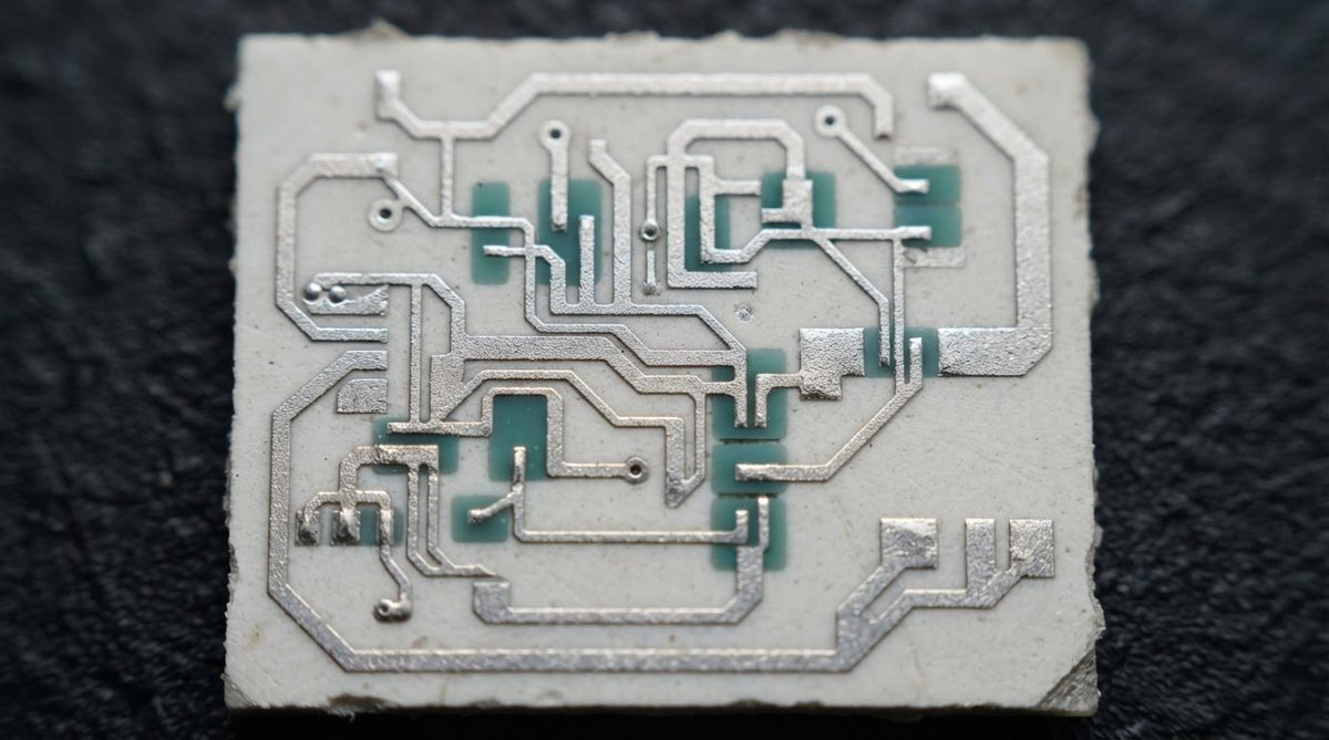
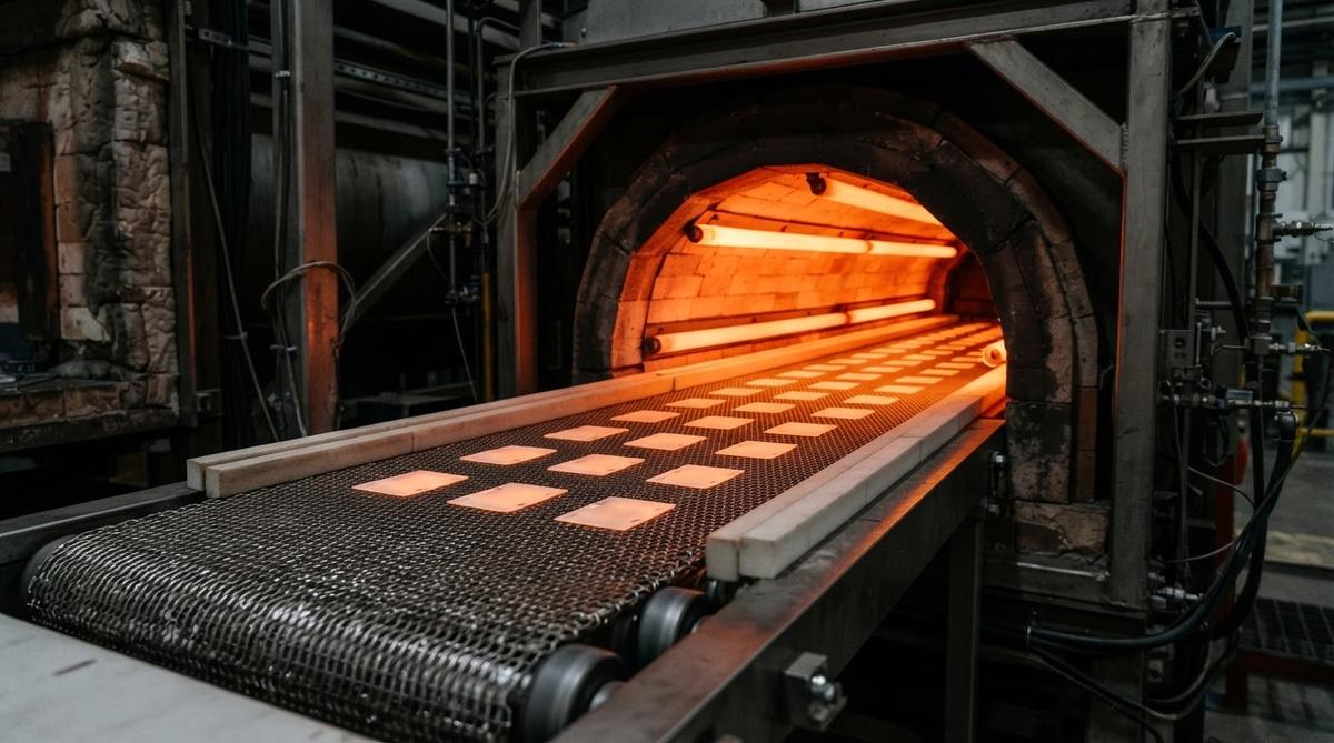
A stainless-steel or polyester mesh, typically 200–400 mesh count, is stretched over a frame and coated with a photosensitive emulsion. The desired circuit pattern is exposed and developed, leaving open areas where paste can pass through. The substrate—commonly 96 % Al₂O₃—is placed on a vacuum chuck beneath the screen. The squeegee pushes paste through the open mesh at a typical speed of 50–150 mm/s, depositing a wet film 20–50 µm thick. After drying at around 125 °C, the part enters a belt furnace for sintering at peak temperatures that depend on the paste chemistry.
Minimum line width achievable with screen printing is roughly 100–125 µm (4–5 mil) for standard production. Finer features require alternative methods such as photolithographic patterning or thin-film sputtering. Fired film thickness is usually 8–15 µm for conductors and 30–50 µm for dielectric layers.
Typical Parameters
| Parameter | Typical Range | Notes |
|---|---|---|
| Mesh count | 200–400 wires/inch | Higher count → finer features, thinner deposit |
| Wet film thickness | 20–50 µm | Before drying |
| Fired conductor thickness | 8–15 µm | Ag, Au, or Ag/Pd pastes |
| Minimum line/space | 100–125 µm | Standard production; tighter with fine-mesh screens |
| Squeegee speed | 50–150 mm/s | Adjusted per paste viscosity |
| Peak firing temperature | 850–1 000 °C | Paste-dependent; per supplier datasheet |
Typical values for commercially available materials, for comparison only. Confirm against the datasheet for your specific paste and mesh.
Where Screen Printing Fits—and Where It Does Not
Screen printing is the workhorse of thick-film ceramic circuit production. It handles conductor traces, resistor elements, dielectric crossovers, and solder mask layers in a single, repeatable process. It is cost-effective for medium-to-high volumes and tolerant of a wide range of paste chemistries.
It is not the right choice when you need line widths below about 75 µm, layer thickness uniformity under ±1 µm, or sub-micron surface-finish control on ceramic PCBs. For those requirements, thin-film sputtering and photolithographic patterning are more appropriate.
FAQ
Is screen printing the same as stencil printing?
They are related but distinct. Screen printing uses a woven mesh with an emulsion pattern; stencil printing uses a solid metal foil with laser-cut apertures. Stencil printing deposits thicker, more uniform layers and is common for solder paste, while screen printing is standard for thick-film pastes on ceramics.
Can screen printing deposit multiple layers?
Yes. Each layer is printed, dried, and sometimes fired before the next layer is applied. Multilayer thick-film circuits routinely stack conductors, dielectrics, and resistors using sequential screen-printing passes.
What paste materials are used?
Common conductor pastes contain silver (Ag), gold (Au), or silver-palladium (Ag/Pd) particles in an organic binder. Resistor pastes use ruthenium oxide (RuO₂) systems. Dielectric pastes are glass- or alumina-filled compositions. Each is matched to the substrate and firing profile.