Power Density Definition: What It Means in PCB Thermal Design
Power density is the thermal power dissipated per unit area (W/cm²) or per unit volume (W/cm³) of an electronic component or circuit board region. Grasping the power density definition is the first step toward selecting the right substrate material. It tells you how concentrated the heat load is. A 10 W device on a 1 cm² footprint has a power density of 10 W/cm²; spread the same 10 W across 10 cm² and the density drops to 1 W/cm².
The formula for areal power density is:
q = P / A
- q — power density (W/cm²)
- P — dissipated power (W)
- A — footprint or active area (cm²)
Power density matters because it drives the temperature rise at the junction. A board’s thermal-resistance path must conduct that flux away fast enough to keep the junction below its rated limit. When power density exceeds roughly 1–2 W/cm², standard FR-4 (thermal conductivity ≈ 0.3 W/mK) struggles to spread heat laterally, and designers turn to metal-core or ceramic substrates.
Why the Power Density Definition Drives Substrate Selection
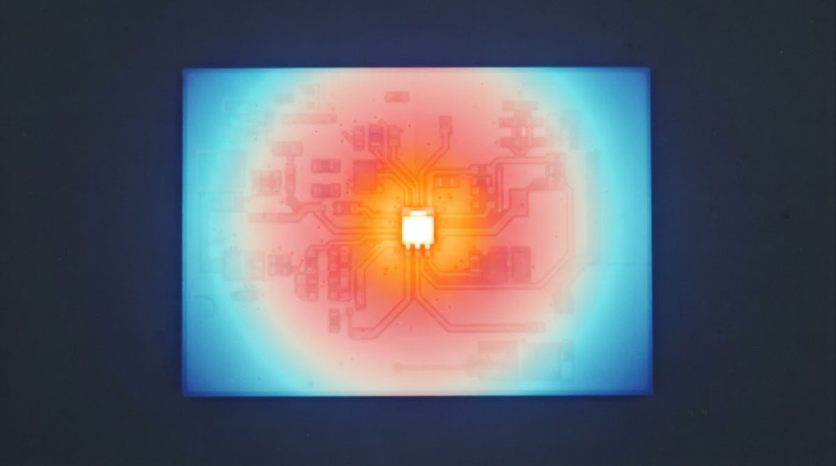
GaN HEMTs, SiC MOSFETs, and high-brightness LEDs routinely push 50–250 W/cm² at die level. At these densities, the substrate directly beneath the die must have high thermal conductivity—aluminum nitride (170–200 W/mK) or silicon nitride (70–90 W/mK)—to avoid a steep thermal gradient. Alumina 96 % (24–28 W/mK) handles moderate power density levels up to roughly 10–20 W/cm² depending on geometry and cooling.
Enter your substrate material, thickness, and dissipated power below to see how power density translates into junction temperature rise for your specific layout.
Worked Example: Applying the Power Density Definition
A 50 W laser diode bar sits on a 0.5 cm × 1.0 cm AlN submount (0.5 cm² footprint).
q = 50 W / 0.5 cm² = 100 W/cm²
At this power density, the conductive temperature drop through a 0.635 mm thick AlN substrate (k ≈ 180 W/mK) is approximately:
ΔT = q × t / k = 100 × 0.0635 / 1.80 ≈ 3.5 °C
The same geometry in 96 % alumina (k ≈ 25 W/mK) would produce roughly 25 °C of drop—often enough to push the junction over its limit.
When Power Density Is Not the Deciding Factor
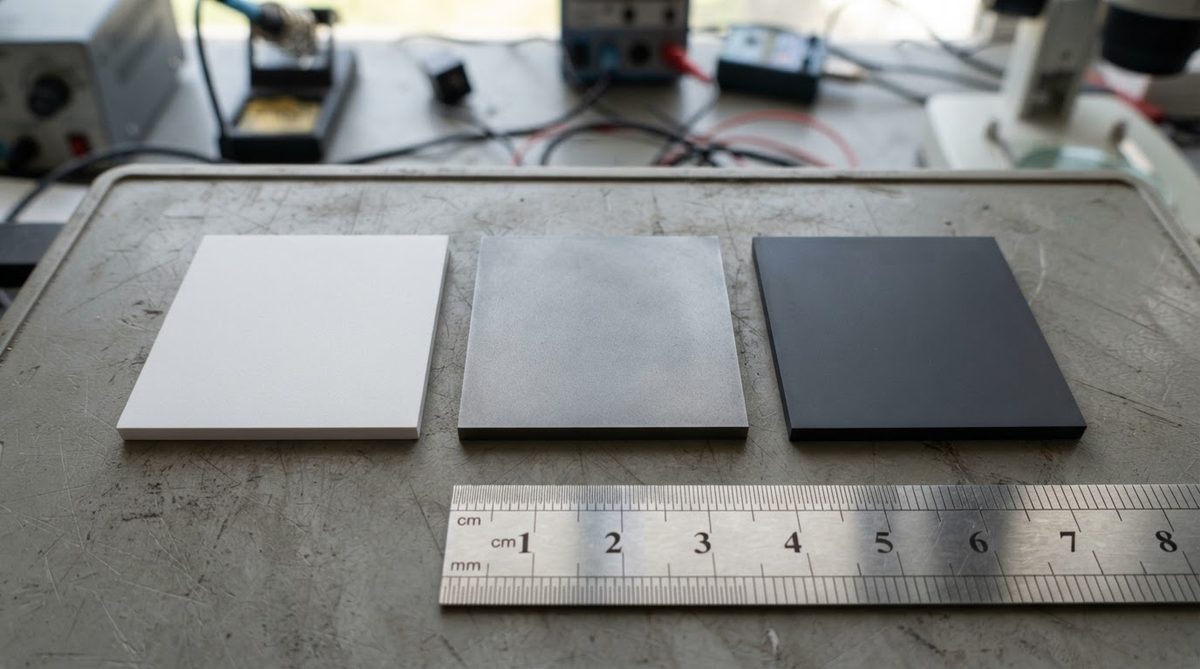
If your board dissipates under 0.5 W/cm² uniformly, FR-4 or a metal-core PCB will usually suffice. Ceramic substrates add cost and are brittle; they earn their place only when thermal, dielectric, or frequency requirements demand them. Always run the thermal numbers before specifying ceramic.
FAQ
What units are used for power density on PCBs?
The most common unit is W/cm². Datasheets for power modules sometimes use W/mm² or W/in². Convert carefully: 1 W/mm² = 100 W/cm².
Is power density the same as heat flux?
In PCB thermal analysis, yes—they are used interchangeably. Both describe watts per unit area flowing through a surface. Strictly, “heat flux” can also refer to radiated or convected energy, but on a substrate the conduction term dominates.
How do I reduce power density without lowering power?
Increase the effective spreading area. Use a larger die-attach pad, add thermal vias beneath the component, or choose a substrate with higher thermal conductivity so heat spreads laterally before reaching the board-level interface.
What power density requires a ceramic substrate?
There is no single threshold. As a guideline, designs above 5–10 W/cm² at the substrate surface benefit from alumina; above 30–50 W/cm², aluminum nitride or silicon nitride is typically justified. The actual limit depends on ambient temperature, cooling method, and allowable junction temperature.