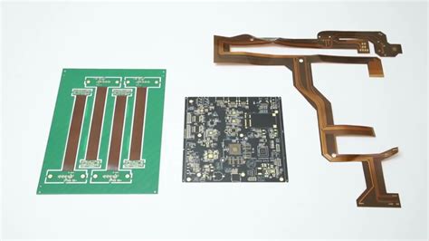
What is a Flex PCB?
A flex PCB, also known as a flexible printed circuit board, is a type of PCB that consists of a thin, flexible substrate made of polymeric materials such as polyimide or polyester. Unlike traditional rigid PCBs, flex PCBs can bend, twist, and conform to various shapes, making them ideal for applications where space is limited or where the device needs to adapt to the contours of the enclosure.
Flex PCBs offer several advantages over rigid PCBs, including:
- Reduced weight and size
- Improved reliability due to reduced interconnections
- Enhanced flexibility and durability
- Ability to withstand vibration and shock
- Increased design freedom and integration possibilities
Flex PCB Manufacturing Process Overview
The flex PCB manufacturing process involves several steps that are similar to those used in the production of rigid PCBs. However, due to the unique properties of flex PCBs, some additional considerations and techniques are employed to ensure the desired flexibility and reliability.
The main steps in the flex PCB manufacturing process are as follows:
- Designing the Flex PCB
- Printing the Circuit Pattern
- Etching the Circuit Pattern
- Laminating the Layers
- Drilling and Cutting
- Surface Finishing
- Electrical Testing and Inspection
- Packaging and Shipping
Let’s explore each of these steps in more detail.

Step 1: Designing the Flex PCB
The first step in the flex PCB manufacturing process is designing the circuit layout. This involves creating a schematic diagram that outlines the electrical connections between components and then translating that schematic into a physical layout using specialized PCB design software.
When designing a flex PCB, several factors need to be considered, such as:
- Bend radius and flexibility requirements
- Material selection (e.g., polyimide, polyester)
- Copper thickness and trace width
- Component placement and orientation
- Shielding and grounding requirements
- Impedance control and signal integrity
Designers must also adhere to the design rules and guidelines provided by the flex PCB manufacturer to ensure manufacturability and reliability.

Step 2: Printing the Circuit Pattern
Once the design is finalized, the next step is to print the circuit pattern onto the flexible substrate. This is typically done using a photolithography process, which involves the following sub-steps:
- Applying a photoresist layer: A light-sensitive polymer called photoresist is applied evenly onto the copper-clad flexible substrate.
- Exposing the photoresist: The photoresist-coated substrate is then exposed to UV light through a photomask that contains the circuit pattern. The areas exposed to UV light become soluble in a developer solution.
- Developing the photoresist: The exposed substrate is immersed in a developer solution, which removes the soluble portions of the photoresist, leaving behind the circuit pattern.

Step 3: Etching the Circuit Pattern
After the circuit pattern is printed onto the substrate, the next step is to etch away the unwanted copper, leaving behind only the desired circuit traces. This is typically done using a chemical etching process, which involves the following sub-steps:
- Immersing the substrate in an etchant solution: The substrate is placed in a bath containing an etchant solution, such as ferric chloride or ammonium persulfate.
- Etching away the unwanted copper: The etchant solution selectively removes the copper that is not protected by the photoresist, leaving behind the desired circuit pattern.
- Stripping the remaining photoresist: After etching, the remaining photoresist is stripped away using a chemical stripper, revealing the final circuit pattern.
Step 4: Laminating the Layers
In many cases, flex PCBs consist of multiple layers that need to be laminated together to form a single, cohesive structure. The lamination process involves the following sub-steps:
- Aligning the layers: The individual layers of the flex PCB are aligned using registration marks to ensure proper positioning.
- Applying adhesive: A thin layer of adhesive, typically an epoxy or acrylic-based material, is applied between the layers to bond them together.
- Pressing and curing: The aligned layers are then pressed together under high temperature and pressure to cure the adhesive and form a strong, reliable bond.
Step 5: Drilling and Cutting
After lamination, the next step is to drill any necessary holes and cut the flex PCB to its final shape. This is typically done using specialized equipment, such as:
- CNC drilling machines: Used to drill precise holes for component mounting and interconnections.
- Laser cutting machines: Used to cut the flex PCB to its final shape with high accuracy and minimal stress on the material.
- Die-cutting machines: Used for high-volume production runs, where a custom die is created to cut the flex PCB to shape.
Step 6: Surface Finishing
To enhance the durability, solderability, and aesthetic appearance of the flex PCB, various surface finishes can be applied. Some common surface finishes include:
- HASL (Hot Air Solder Leveling): A tin-lead alloy is applied to the exposed copper traces and pads, providing a solderable surface.
- ENIG (Electroless Nickel Immersion Gold): A thin layer of nickel is deposited onto the copper, followed by a thin layer of gold, providing excellent solderability and corrosion resistance.
- OSP (Organic Solderability Preservative): A thin, organic coating is applied to the exposed copper, protecting it from oxidation and enhancing solderability.
Step 7: Electrical Testing and Inspection
Before the flex PCB is packaged and shipped, it undergoes rigorous electrical testing and inspection to ensure its functionality and quality. This involves:
- Continuity testing: Verifying that all electrical connections are intact and there are no open circuits.
- Insulation resistance testing: Measuring the resistance between adjacent traces to ensure adequate insulation.
- Visual inspection: Examining the flex PCB for any visible defects, such as misaligned layers, scratches, or contaminants.
- Functional testing: Verifying that the flex PCB performs as intended in its final application.
Step 8: Packaging and Shipping
Once the flex PCB has passed all the necessary tests and inspections, it is packaged and shipped to the customer. Proper packaging is essential to protect the flex PCB from damage during transport and storage. This may involve the use of:
- ESD (Electrostatic Discharge) protection: Flex PCBs are susceptible to damage from static electricity, so they are typically packaged in ESD-safe materials.
- Moisture barrier bags: To prevent moisture from affecting the flex PCB during storage, it may be sealed in a moisture barrier bag with desiccants.
- Rigid packaging: For added protection during shipping, flex PCBs may be placed in rigid boxes or containers.
Key Considerations in Flex PCB Manufacturing
When manufacturing flex PCBs, several key considerations need to be taken into account to ensure a high-quality, reliable product:
Material Selection
Choosing the right materials for a flex PCB is critical to its performance and durability. The most common base materials used in flex PCBs are:
- Polyimide: Known for its excellent thermal stability, chemical resistance, and mechanical strength, polyimide is the most widely used base material for flex PCBs.
- Polyester: While not as heat-resistant as polyimide, polyester offers good flexibility and is often used in less demanding applications.
The copper foil used in flex PCBs also comes in various thicknesses, typically ranging from 9 to 70 microns (µm). Thinner copper foils offer better flexibility but may have limitations in terms of current-carrying capacity.
| Base Material | Thickness (µm) | Temperature Range (°C) | Key Properties |
|---|---|---|---|
| Polyimide | 25 – 125 | -269 to +400 | High heat resistance, good chemical resistance, excellent mechanical strength |
| Polyester | 50 – 125 | -40 to +150 | Good flexibility, lower cost compared to polyimide |
Bend Radius and Flexibility
One of the key advantages of flex PCBs is their ability to bend and flex without damaging the circuit traces. However, designers must consider the minimum bend radius and the number of flex cycles required for the application.
The minimum bend radius is determined by factors such as the thickness of the base material, the copper foil thickness, and the presence of any stiffeners or reinforcements. Exceeding the minimum bend radius can lead to cracks in the copper traces or delamination of the layers.
The number of flex cycles refers to the number of times the flex PCB is expected to be bent or flexed during its lifetime. This is an important consideration when choosing materials and designing the circuit layout to ensure long-term reliability.
| Copper Thickness (µm) | Minimum Bend Radius (mm) |
|---|---|
| 9 | 0.8 |
| 18 | 1.6 |
| 35 | 3.2 |
| 70 | 6.4 |
Shielding and Grounding
Flex PCBs often operate in close proximity to other electronic components or are exposed to electromagnetic interference (EMI). To mitigate these issues, proper shielding and grounding techniques must be employed.
Shielding can be achieved by incorporating conductive layers, such as copper foil or conductive inks, into the flex PCB Stack-up. These layers act as a barrier to block EMI from affecting sensitive circuits.
Grounding is essential to provide a stable reference point for the circuit and to prevent the build-up of static charges. Designers must carefully consider the placement of ground planes and the use of ground vias to ensure proper grounding throughout the flex PCB.
Impedance Control and Signal Integrity
As with rigid PCBs, maintaining proper impedance control and signal integrity is crucial for high-speed flex PCB designs. Factors such as trace width, spacing, and dielectric thickness must be carefully calculated and controlled to ensure that signals propagate correctly and without distortion.
Designers may also need to incorporate techniques such as differential signaling, termination, and length matching to maintain signal integrity in flex PCB designs.
Conclusion
Flex PCB manufacturing is a complex process that requires careful consideration of design, materials, and processing techniques to ensure a high-quality, reliable product. By understanding the steps involved in the manufacturing process and the key considerations for flex PCB design, engineers and designers can create innovative, compact, and robust electronic devices that leverage the unique capabilities of flex PCBs.
As the demand for smaller, lighter, and more flexible electronic devices continues to grow, the importance of flex PCBs in the electronics industry will only continue to increase. By staying up-to-date with the latest advancements in flex PCB manufacturing and design, companies can remain competitive and deliver cutting-edge products to their customers.
Frequently Asked Questions (FAQ)
1. What are the advantages of using flex PCBs over rigid PCBs?
Flex PCBs offer several advantages over rigid PCBs, including reduced weight and size, improved reliability due to fewer interconnections, enhanced flexibility and durability, ability to withstand vibration and shock, and increased design freedom and integration possibilities.
2. What are the most common base materials used in flex PCBs?
The most common base materials used in flex PCBs are polyimide and polyester. Polyimide is known for its excellent thermal stability, chemical resistance, and mechanical strength, while polyester offers good flexibility and is often used in less demanding applications.
3. What is the minimum bend radius for a flex PCB?
The minimum bend radius for a flex PCB depends on factors such as the thickness of the base material, the copper foil thickness, and the presence of any stiffeners or reinforcements. Generally, thinner copper foils and base materials allow for smaller bend radii.
4. How can shielding and grounding be achieved in flex PCBs?
Shielding in flex PCBs can be achieved by incorporating conductive layers, such as copper foil or conductive inks, into the flex PCB stack-up. Grounding is essential to provide a stable reference point for the circuit and can be achieved through the careful placement of ground planes and the use of ground vias.
5. What are some key considerations for maintaining signal integrity in flex PCB designs?
To maintain signal integrity in flex PCB designs, factors such as trace width, spacing, and dielectric thickness must be carefully calculated and controlled. Techniques such as differential signaling, termination, and length matching may also be incorporated to ensure that signals propagate correctly and without distortion.


Leave a Reply