Introduction to PCB Stack-up
Printed Circuit Board (PCB) stack-up refers to the arrangement of copper layers and insulating materials that make up a PCB. A well-designed stack-up ensures proper signal integrity, power distribution, and manufacturability. As the complexity of electronic devices increases, so does the need for multi-layer PCBs. In this article, we will focus on the guidelines for creating a 10-layer PCB stack-up.
The Importance of PCB Stack-up Design
PCB stack-up design is crucial because it directly affects the performance and reliability of the final product. A properly designed stack-up can:
- Minimize signal integrity issues, such as crosstalk and electromagnetic interference (EMI)
- Ensure proper power distribution and reduce voltage drop
- Improve thermal management
- Enhance manufacturability and reduce production costs
Factors to Consider When Designing a 10-Layer PCB Stack-up
When designing a 10-layer PCB stack-up, several factors must be taken into account to ensure optimal performance and manufacturability.
1. Material Selection
The choice of materials for your PCB stack-up is critical. The most common materials used in PCB fabrication are:
- FR-4: A flame-retardant, glass-reinforced epoxy laminate material widely used in PCB production
- High-Tg FR-4: A variant of FR-4 with improved thermal stability and lower dielectric loss
- Isola 370HR: A high-performance material with low dielectric constant and low dissipation factor
- Rogers 4003C: A high-frequency laminate material with excellent electrical properties
Consider the electrical, thermal, and mechanical properties of each material when making your selection.
2. Layer Arrangement
A typical 10-layer PCB stack-up consists of the following layers:
| Layer | Description |
|---|---|
| 1 | Top Signal Layer |
| 2 | Ground Plane |
| 3 | Signal Layer |
| 4 | Power Plane |
| 5 | Signal Layer |
| 6 | Signal Layer |
| 7 | Power Plane |
| 8 | Signal Layer |
| 9 | Ground Plane |
| 10 | Bottom Signal Layer |
This arrangement provides a balance between signal integrity, power distribution, and EMI reduction.
3. Trace Width and Spacing
Trace width and spacing are critical parameters in PCB design. They affect signal integrity, impedance control, and current-carrying capacity. When designing a 10-layer PCB stack-up, consider the following guidelines:
- Use appropriate trace widths based on the current requirements of your design
- Maintain consistent trace widths and spacing within each layer to ensure uniform impedance
- Follow the manufacturer’s recommended trace width and spacing guidelines for your chosen materials
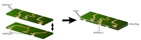
4. Via Design
Vias are essential for interconnecting different layers in a multi-layer PCB. When designing vias for a 10-layer PCB stack-up, keep the following points in mind:
- Use appropriate via sizes and drill diameters based on your design requirements and manufacturability constraints
- Minimize the number of vias to reduce manufacturing costs and improve signal integrity
- Use via stitching around high-speed signals to reduce EMI and improve signal quality
5. Impedance Control
Impedance control is crucial for maintaining signal integrity in high-speed designs. When designing a 10-layer PCB stack-up, consider the following:
- Calculate the required impedance for your design based on the signal speed and rise time
- Adjust trace widths, spacing, and dielectric thickness to achieve the desired impedance
- Use differential pair routing for high-speed signals to minimize crosstalk and EMI

Example of a 10-Layer PCB Stack-up
Here is an example of a 10-layer PCB stack-up using Isola 370HR material:
| Layer | Material | Thickness (mm) | Layer Type |
|---|---|---|---|
| 1 | Isola 370HR | 0.036 | Top Signal Layer |
| 2 | Isola 370HR | 0.18 | Ground Plane |
| 3 | Isola 370HR | 0.11 | Signal Layer |
| 4 | Isola 370HR | 0.18 | Power Plane |
| 5 | Isola 370HR | 0.11 | Signal Layer |
| 6 | Isola 370HR | 0.11 | Signal Layer |
| 7 | Isola 370HR | 0.18 | Power Plane |
| 8 | Isola 370HR | 0.11 | Signal Layer |
| 9 | Isola 370HR | 0.18 | Ground Plane |
| 10 | Isola 370HR | 0.036 | Bottom Signal Layer |
This stack-up provides a total thickness of 1.262 mm and offers a good balance between signal integrity, power distribution, and manufacturability.

Design Considerations for High-Speed Signals
When designing a 10-layer PCB stack-up for high-speed applications, there are several additional factors to consider:
1. Signal Routing
- Route high-speed signals on inner layers to minimize EMI and crosstalk
- Use differential pair routing for high-speed signals
- Avoid routing high-speed signals near the board edges to reduce EMI
2. Power Distribution Network (PDN)
- Use dedicated power and ground planes to provide a low-impedance power distribution network
- Place decoupling capacitors close to the power pins of high-speed devices
- Use multiple vias to connect decoupling capacitors to the power and ground planes
3. Shielding
- Use ground planes to shield sensitive signals from EMI
- Implement via stitching around high-speed signals to create a Faraday cage and reduce EMI
- Consider using shielded connectors for high-speed interfaces

Manufacturing Considerations
When designing a 10-layer PCB stack-up, it is essential to consider the manufacturing process to ensure the best possible outcome.
1. Copper Weight
- Use appropriate copper weights for each layer based on the current requirements and manufacturability constraints
- Consult with your PCB manufacturer to determine the available copper weights and their recommendations
2. Drilling and Plating
- Use appropriate drill sizes and aspect ratios to ensure proper plating and minimize manufacturing issues
- Consult with your PCB manufacturer to determine their drilling and plating capabilities and guidelines
3. Solder Mask and Silkscreen
- Use appropriate solder mask and silkscreen materials based on your design requirements and manufacturing constraints
- Ensure proper solder mask and silkscreen clearances around components and vias
Frequently Asked Questions (FAQ)
-
Q: What is the purpose of having multiple layers in a PCB?
A: Multiple layers in a PCB allow for more complex routing, better signal integrity, and improved power distribution. They also help reduce the overall size of the PCB. -
Q: How do I choose the right materials for my 10-layer PCB stack-up?
A: When choosing materials for your 10-layer PCB stack-up, consider the electrical, thermal, and mechanical properties required for your application. Consult with your PCB manufacturer and refer to material datasheets to make an informed decision. -
Q: What is the importance of impedance control in a 10-layer PCB stack-up?
A: Impedance control is crucial for maintaining signal integrity in high-speed designs. It helps minimize signal reflections, crosstalk, and EMI, ensuring proper functioning of the electronic device. -
Q: How can I minimize EMI in my 10-layer PCB stack-up?
A: To minimize EMI in your 10-layer PCB stack-up, use ground planes for shielding, implement via stitching around high-speed signals, and consider using shielded connectors for high-speed interfaces. Additionally, route high-speed signals on inner layers and use differential pair routing. -
Q: What should I consider when selecting drill sizes for my 10-layer PCB stack-up?
A: When selecting drill sizes for your 10-layer PCB stack-up, consider the required aspect ratios for proper plating and the capabilities of your PCB manufacturer. Use appropriate drill sizes to minimize manufacturing issues and ensure reliable connections between layers.
Conclusion
Designing a 10-layer PCB stack-up requires careful consideration of various factors, including material selection, layer arrangement, trace width and spacing, via design, and impedance control. By following the guidelines presented in this article and working closely with your PCB manufacturer, you can create a robust and reliable 10-layer PCB stack-up that meets your design requirements and ensures optimal performance.


Leave a Reply