What is PCB Drilling?
PCB drilling is the process of creating holes in a printed circuit board to accommodate electronic components, facilitate electrical connections between layers, and provide mounting points for the board itself. These holes are essential for the proper functioning and reliability of the PCB.
Types of Holes in PCBs
There are three main types of holes found in PCBs:
-
Component Holes: These holes are drilled to accommodate the leads of through-hole components, such as resistors, capacitors, and integrated circuits.
-
Via Holes: Vias are small holes that connect different layers of a multi-layer PCB, allowing electrical signals to pass between layers.
-
Mounting Holes: These holes are used to secure the PCB to an enclosure or chassis using screws or other fasteners.
Importance of Precise PCB Drilling
Accurate and precise drilling is crucial for the proper functioning and reliability of a PCB. Poorly drilled holes can lead to various issues, such as:
- Misaligned or improperly seated components
- Poor electrical connections between layers
- Mechanical stress and weakness in the board
- Increased risk of short circuits and signal integrity issues
To ensure the best performance and longevity of a PCB, it is essential to maintain tight tolerances and high-quality drilling throughout the manufacturing process.
PCB Drilling Techniques
There are several techniques used for drilling PCBs, each with its advantages and limitations. The choice of drilling method depends on factors such as the required hole size, precision, throughput, and cost.
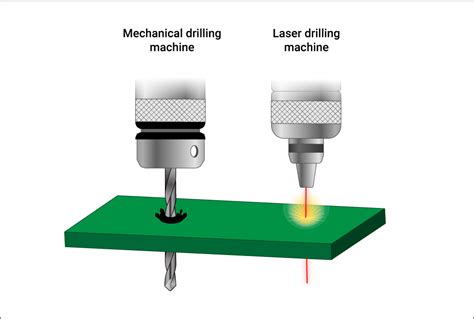
Mechanical Drilling
Mechanical drilling is the most common method for creating holes in PCBs. It involves using high-speed drill bits, typically made of carbide or diamond-coated materials, to physically remove material from the board.
Advantages of Mechanical Drilling
- Versatility in hole sizes and shapes
- Suitable for a wide range of PCB materials
- Relatively low cost compared to other methods
- Well-established and widely available technology
Limitations of Mechanical Drilling
- Limited by the size of the drill bit, making it challenging to create very small holes
- Slower than some other methods, especially for high-density boards
- Drill bits are subject to wear and breakage, requiring regular replacement
- May cause localized stress and delamination around the drilled hole
Laser Drilling
Laser drilling uses a focused laser beam to vaporize the PCB material, creating precise holes without physical contact. This method is particularly suitable for creating small, high-density holes in Multi-layer Boards.
Advantages of Laser Drilling
- Capable of creating very small holes (down to 50 microns or less)
- High precision and repeatability
- No physical contact with the board, reducing mechanical stress
- Fast drilling speed, especially for high-density boards
- Minimal wear and tear on the drilling equipment
Limitations of Laser Drilling
- Higher cost compared to mechanical drilling
- Limited material compatibility (some materials may not be suitable for laser drilling)
- Potential for thermal damage to the surrounding area
- May require specialized equipment and skilled operators
Punching
Punching is a method that uses a die and punch set to create holes in the PCB material. This technique is typically used for larger holes and is well-suited for high-volume production.
Advantages of Punching
- Fast and efficient for large holes and high-volume production
- Consistent hole quality and repeatability
- Lower cost per hole compared to drilling, especially for larger quantities
- Minimal stress and delamination around the punched hole
Limitations of Punching
- Limited to larger hole sizes (typically 0.8 mm or larger)
- Requires custom tooling for each hole size and shape
- Higher initial tooling costs compared to drilling
- Less flexible than drilling for quick design changes or prototyping

Challenges in PCB Drilling
Despite advancements in drilling technologies and techniques, several challenges remain in the PCB drilling process. Addressing these challenges is crucial for maintaining the quality and reliability of the final product.
Hole Size and Aspect Ratio
As electronic devices continue to shrink and become more complex, the demand for smaller and more densely packed PCBs increases. This trend poses challenges for PCB drilling, particularly in terms of hole size and aspect ratio (the ratio of hole depth to diameter).
| Hole Size | Typical Application | Drilling Method |
|---|---|---|
| > 0.8 mm | Through-hole components, mounting holes | Mechanical drilling, punching |
| 0.3 – 0.8 mm | Small through-hole components, vias | Mechanical drilling, laser drilling |
| < 0.3 mm | High-density vias, micro-vias | Laser drilling |
Creating small holes with high aspect ratios requires specialized equipment, precise control, and optimized process parameters to ensure hole quality and minimize defects.
Material Compatibility
PCBs can be made from a variety of materials, each with its own properties and challenges for drilling. Some common PCB materials include:
- FR-4 (glass-reinforced epoxy laminate)
- Polyimide
- PTFE (Teflon)
- Ceramic
Each material may require specific drilling techniques, tools, and parameters to achieve the desired hole quality and minimize damage to the board. For example, some materials may be more prone to delamination or burring during drilling, requiring careful control of feed rates and spindle speeds.
Drill Bit Wear and Breakage
In mechanical drilling, the drill bits are subject to wear and tear due to the abrasive nature of the PCB materials. As the drill bits wear, the hole quality may degrade, leading to issues such as:
- Oversized or undersized holes
- Rough hole walls
- Burring or debris around the hole
- Misaligned or non-perpendicular holes
Regular inspection, maintenance, and replacement of drill bits are essential to maintain consistent hole quality throughout the production run. Additionally, optimizing drilling parameters, such as feed rates and spindle speeds, can help extend drill bit life and minimize breakage.
Throughput and Efficiency
In high-volume PCB Production, drilling throughput and efficiency are critical factors for meeting production targets and controlling costs. Balancing hole quality, drilling speed, and tool life can be challenging, particularly for complex boards with a large number of holes.
To improve drilling efficiency, manufacturers may employ various strategies, such as:
- Multi-spindle drilling machines for parallel processing
- High-speed spindles and optimized feed rates
- Automated tool change systems for rapid drill bit replacement
- Intelligent drilling path optimization to minimize travel time between holes
Adopting advanced drilling technologies, such as laser drilling for small holes, can also help improve overall throughput and efficiency in PCB production.

Best Practices for PCB Drilling
To achieve the best results in PCB drilling, manufacturers should follow several best practices and guidelines:
-
Design for Manufacturability (DFM): Collaborate with PCB designers to ensure that the board layout is optimized for drilling, considering factors such as hole sizes, spacing, and Layer Stack-Up.
-
Material Selection: Choose PCB materials that are compatible with the intended drilling method and application requirements, considering factors such as thermal stability, mechanical strength, and electrical properties.
-
Equipment Maintenance: Regularly inspect, maintain, and calibrate drilling equipment to ensure consistent performance and hole quality. This includes cleaning, lubricating, and replacing worn or damaged components as needed.
-
Process Optimization: Fine-tune drilling parameters, such as spindle speed, feed rate, and depth of cut, to achieve the best balance between hole quality, throughput, and tool life. Use statistical process control (SPC) techniques to monitor and maintain process stability.
-
Quality Control: Implement a robust quality control system to monitor and verify hole quality throughout the production process. This may include visual inspection, automated optical inspection (AOI), and destructive testing of sample boards.
-
Continuous Improvement: Foster a culture of continuous improvement, encouraging operators and engineers to identify and address issues, optimize processes, and adopt new technologies and best practices as they become available.
By following these best practices and staying current with the latest advancements in PCB drilling technology, manufacturers can ensure high-quality, reliable, and cost-effective PCB production.

Frequently Asked Questions (FAQ)
-
What is the most common method for drilling PCBs?
The most common method for drilling PCBs is mechanical drilling, which uses high-speed drill bits to remove material from the board. -
What are the advantages of laser drilling for PCBs?
Laser drilling offers several advantages, including the ability to create very small holes (down to 50 microns or less), high precision and repeatability, minimal mechanical stress on the board, and fast drilling speeds for high-density boards. -
What challenges are associated with drilling small holes in PCBs?
Drilling small holes in PCBs can be challenging due to the high aspect ratios (hole depth to diameter) required. This necessitates specialized equipment, precise control, and optimized process parameters to ensure hole quality and minimize defects. -
How can manufacturers improve drilling efficiency in high-volume PCB production?
To improve drilling efficiency, manufacturers can employ strategies such as multi-spindle drilling machines, high-speed spindles and optimized feed rates, automated tool change systems, and intelligent drilling path optimization. Adopting advanced drilling technologies, such as laser drilling for small holes, can also help improve overall throughput and efficiency. -
What are some best practices for achieving high-quality PCB drilling?
Best practices for high-quality PCB drilling include designing for manufacturability (DFM), selecting compatible materials, maintaining and calibrating equipment regularly, optimizing drilling parameters, implementing robust quality control systems, and fostering a culture of continuous improvement.
In conclusion, PCB drilling is a critical process in the manufacture of printed circuit boards, enabling the creation of holes for component assembly, electrical connections, and mechanical mounting. By understanding the various drilling techniques, challenges, and best practices, manufacturers can ensure the production of high-quality, reliable PCBs that meet the ever-increasing demands of modern electronics. As technology continues to advance, staying current with the latest developments in PCB drilling will be essential for success in this rapidly evolving industry.


Leave a Reply