Introduction to Flexible PCBs
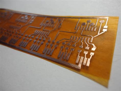
Flexible printed circuit boards, also known as flex circuits or flexible PCBs, are a type of printed circuit board that is designed to be flexible and bendable. Unlike traditional rigid PCBs, flexible PCBs can conform to different shapes and fit into tight spaces, making them ideal for applications where space is limited or where the PCB needs to move or flex during operation.
Flexible PCBs are widely used in a variety of industries, including consumer electronics, medical devices, aerospace, and automotive. They offer several advantages over rigid PCBs, such as:
- Reduced weight and space requirements
- Improved reliability and durability
- Increased design flexibility
- Better shock and vibration resistance
In this article, we will explore the process of making a DIY flexible PCB, including the materials and tools required, the design considerations, and the step-by-step instructions for fabricating a flexible PCB at home.
Materials and Tools Required
Before we dive into the process of making a flexible PCB, let’s take a look at the materials and tools you will need:
Materials
- Copper-clad flexible substrate (e.g. Pyralux or Kapton)
- Photoresist film or spray
- Developer solution
- Etching solution (e.g. ferric chloride or ammonium persulfate)
- Solder mask ink or film
- Silkscreen ink or film
- Solder paste
- Components for your circuit
Tools
- Laser printer or photoplotter
- UV exposure unit
- Etching tank or tray
- Solder mask and silkscreen application tools
- Soldering iron and solder wire
- Multimeter for testing

Designing Your Flexible PCB
The first step in making a flexible PCB is to design your circuit. You can use any PCB design software, such as Eagle, KiCad, or Altium Designer, to create your schematic and layout.
When designing a flexible PCB, there are several considerations you need to keep in mind:
Bend Radius
Flexible PCBs are designed to bend and flex, but there is a limit to how much they can bend without damaging the traces or components. The minimum bend radius depends on the thickness of the substrate and the copper traces. As a general rule, the minimum bend radius should be at least 10 times the thickness of the substrate.
Trace Width and Spacing
The width and spacing of the traces on a flexible PCB are critical to ensure proper flexibility and reliability. Traces that are too thin or too close together can break or short-circuit when the PCB is flexed. The minimum trace width and spacing depend on the manufacturing process and the requirements of your circuit.
Here is a table showing some common trace width and spacing guidelines for flexible PCBs:
| Trace Width (mm) | Minimum Spacing (mm) |
|---|---|
| 0.2 | 0.2 |
| 0.25 | 0.25 |
| 0.3 | 0.3 |
| 0.4 | 0.4 |
Coverlay
Coverlay is a thin, flexible film that is laminated over the copper traces to protect them from damage and provide electrical insulation. Coverlay is typically made from polyimide or polyester material and comes in different thicknesses and colors.
When designing your flexible PCB, you need to consider the placement and size of the coverlay openings for the components and connectors. The coverlay openings should be slightly larger than the component pads to allow for proper alignment and soldering.
Stiffeners
Stiffeners are rigid materials, such as FR4 or aluminum, that are bonded to certain areas of the flexible PCB to provide mechanical support and prevent excessive bending. Stiffeners are commonly used in areas where connectors or heavy components are mounted.
When designing your flexible PCB, you need to consider the placement and size of the stiffeners to ensure proper support and avoid interfering with the flexibility of the PCB.

Fabricating Your Flexible PCB
Once you have designed your flexible PCB, the next step is to fabricate it. Here is a step-by-step guide to making your own flexible PCB at home:
Step 1: Print the Circuit Pattern
The first step is to print the circuit pattern onto a transparency film using a laser printer or photoplotter. Make sure the printed pattern is sharp and has high contrast.
Step 2: Expose the Photoresist
Next, you need to apply a layer of photoresist onto the copper-clad flexible substrate. You can use either a dry film photoresist or a liquid photoresist spray. Follow the manufacturer’s instructions for application and drying times.
Once the photoresist is dry, place the transparency film with the printed circuit pattern onto the photoresist and expose it to UV light for the recommended time. The UV light will harden the photoresist in the areas that are not covered by the black ink on the transparency film.
Step 3: Develop the Photoresist
After exposure, remove the transparency film and develop the photoresist using a developer solution. The developer will dissolve the unhardened photoresist, leaving behind the circuit pattern on the copper.
Step 4: Etch the Copper
Next, you need to etch away the unwanted copper using an etching solution, such as ferric chloride or ammonium persulfate. Place the PCB in the etching tank or tray and agitate it gently until all the exposed copper is removed. This can take anywhere from a few minutes to an hour, depending on the strength of the etching solution and the thickness of the copper.
Step 5: Remove the Photoresist
Once the etching is complete, remove the remaining photoresist using a solvent or stripper solution. This will leave behind the copper traces in the desired circuit pattern.
Step 6: Apply Solder Mask and Silkscreen
To protect the copper traces and improve the appearance of the PCB, you can apply a layer of solder mask and silkscreen. Solder mask is a thin, heat-resistant coating that covers the copper traces, while silkscreen is used to print text and symbols onto the PCB.
You can apply solder mask and silkscreen using either a liquid ink or a dry film. Follow the manufacturer’s instructions for application and curing.
Step 7: Cut and Drill the PCB
Once the solder mask and silkscreen are cured, you need to cut the PCB to the desired shape and size using a scissors or a cutting tool. You may also need to drill holes for mounting or connecting the components.
Step 8: Solder the Components
Finally, you can solder the components onto the PCB using a soldering iron and solder wire. Make sure to use the appropriate solder type and temperature for the components and the substrate material.

Testing and Troubleshooting
After assembling your flexible PCB, it’s important to test it thoroughly to ensure proper functionality and reliability. Here are some common testing and troubleshooting techniques:
Continuity Testing
Use a multimeter to check the continuity of the traces and connections. Make sure there are no shorts or open circuits.
Functional Testing
Power up the PCB and test its functionality using the appropriate test equipment or software. Make sure all the components are working as expected.
Visual Inspection
Inspect the PCB visually for any defects or damage, such as cracks, delamination, or burnt components. Use a magnifying glass or microscope for detailed inspection.
Flexibility Testing
Flex the PCB gently to ensure it can bend without damaging the traces or components. Make sure the bend radius is within the design specifications.
If you encounter any issues during testing, try to isolate the problem by testing individual components or sections of the PCB. Use the schematic and layout diagrams to trace the signal paths and identify potential points of failure.
FAQ
Can I use any type of flexible substrate for making a flexible PCB?
No, you need to use a copper-clad flexible substrate that is specifically designed for PCB Fabrication, such as Pyralux or Kapton. These substrates have a thin layer of copper bonded to a flexible polymer material.
What is the minimum feature size I can achieve with a DIY flexible PCB?
The minimum feature size depends on the resolution of your printer or photoplotter, as well as the etching process. With a laser printer and standard etching techniques, you can typically achieve a minimum trace width and spacing of around 0.2-0.3mm.
How do I choose the right thickness for my flexible PCB?
The thickness of your flexible PCB depends on the mechanical and electrical requirements of your application. Thinner substrates are more flexible but have lower current carrying capacity and are more prone to damage. Thicker substrates are more robust but less flexible. A common thickness for flexible PCBs is around 0.1-0.3mm.
Can I use the same components for flexible PCBs as for rigid PCBs?
In general, yes, you can use the same components for flexible PCBs as for rigid PCBs. However, you need to pay attention to the mechanical stress and strain on the components during flexing. Some components, such as large capacitors or connectors, may require additional support or strain relief to prevent damage.
How do I ensure the reliability and durability of my flexible PCB?
To ensure the reliability and durability of your flexible PCB, you need to follow good design and manufacturing practices, such as:
- Using the appropriate substrate material and thickness for your application
- Following the recommended trace width and spacing guidelines
- Applying coverlay and stiffeners in critical areas
- Using strain relief and support for heavy components
- Testing the PCB thoroughly for functionality and flexibility
- Protecting the PCB from environmental factors, such as moisture, heat, and chemicals
By following these guidelines and best practices, you can create a high-quality, reliable, and durable flexible PCB for your project.
Conclusion
In this article, we have explored the process of making a DIY flexible PCB, including the materials and tools required, the design considerations, and the step-by-step instructions for fabricating a flexible PCB at home.
Flexible PCBs offer several advantages over traditional rigid PCBs, such as reduced weight and space requirements, improved reliability and durability, increased design flexibility, and better shock and vibration resistance. However, designing and fabricating a flexible PCB requires careful consideration of factors such as bend radius, trace width and spacing, coverlay, and stiffeners.
By following the guidelines and best practices outlined in this article, you can create a high-quality, reliable, and durable flexible PCB for your project. Whether you are a hobbyist or a professional, making your own flexible PCB can be a rewarding and cost-effective way to bring your electronic designs to life.


Leave a Reply