Ceramic PCB panel size is limited by the sintered substrate blank, not by a continuous laminate roll. Most alumina (Al₂O₃) production panels top out around 114 × 114 mm (4.5″ × 4.5″) or 190 × 140 mm (7.5″ × 5.5″), while aluminum nitride (AlN) and silicon nitride (Si₃N₄) panels are typically smaller—often 114 × 114 mm or less. These constraints directly affect your array layout, per-unit cost, and minimum order economics.
Standard Ceramic PCB Panel Sizes by Material
Raw ceramic substrates are pressed and sintered in discrete sizes. Unlike FR-4, where a manufacturer can cut from a 457 × 610 mm (18″ × 24″) panel or larger, ceramic blanks are fixed. The table below lists the sizes you will encounter most often when quoting production work.
| Material | Common Panel Sizes (mm) | Max Thickness Range (mm) | Notes |
|---|---|---|---|
| Al₂O₃ 96% | 114 × 114, 139 × 190, 152 × 152 | 0.25–2.0 | Widest selection; some suppliers offer up to 190 × 240 |
| Al₂O₃ 99.6% | 114 × 114, 139 × 190 | 0.25–1.0 | Fewer large-format options than 96% |
| AlN | 114 × 114, up to 140 × 190 (limited) | 0.25–1.5 | Larger blanks available from select suppliers (Maruwa, Kyocera) |
| Si₃N₄ | 114 × 114, some 139 × 190 | 0.25–0.635 | Thinner substrates; large panels are rare and expensive |
Typical values from major substrate manufacturers (CoorsTek, Kyocera, Maruwa). Confirm dimensions against the specific grade datasheet before design.
For a detailed list of blank substrate dimensions, see standard ceramic substrate sizes.
Why Ceramic Panels Are Smaller Than FR-4
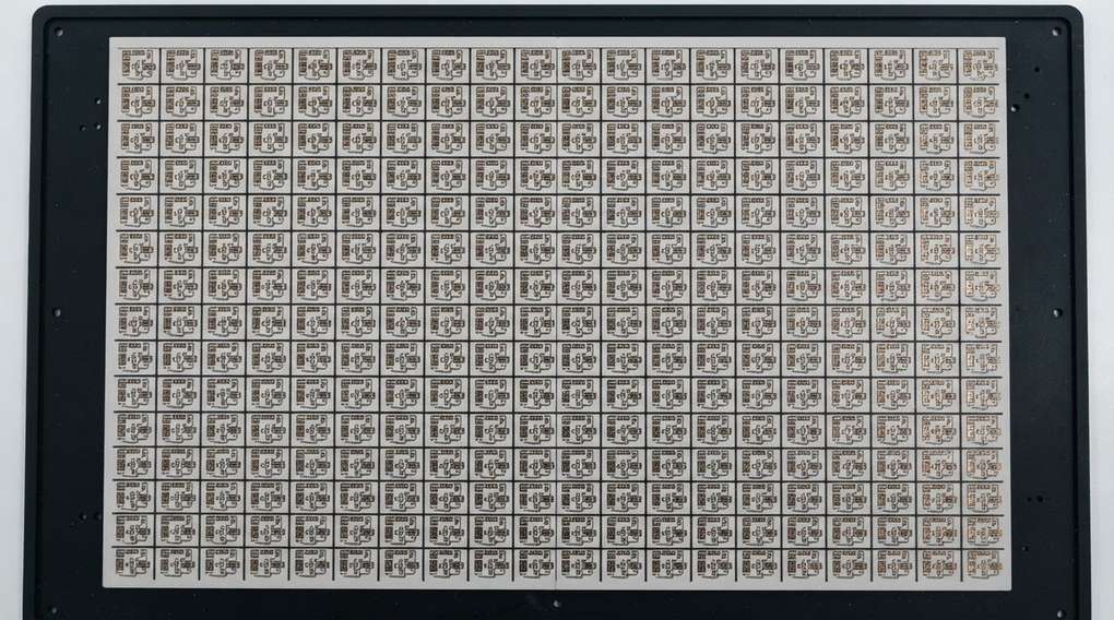
FR-4 starts as a glass-fiber prepreg laminated with copper foil in continuous or semi-continuous processes. Panels of 457 × 610 mm or even 610 × 915 mm are standard. Ceramic substrates follow a completely different path: powder is pressed into a green body, then sintered at 1,500–1,900 °C. Shrinkage during sintering is 15–20%, and maintaining flatness and uniform density across a large area becomes exponentially harder as panel size grows.
Warpage tolerance for a 114 × 114 mm alumina blank is typically ≤ 0.1 mm (per CoorsTek ADS-96R datasheet). Scale that blank up to 190 × 240 mm and achievable warpage may double, which tightens your downstream ceramic PCB production process tolerances for metallization, photolithography, and reflow.
Working Area vs. Panel Size
The working area is always smaller than the panel. You lose material to edge exclusion zones, tooling holes, fiducials, and snap-off tabs (if panelized). A practical rule of thumb:
- Edge exclusion: 2–3 mm per side for DPC and thin-film processes; 1.5–2 mm for thick-film.
- Fiducials and tooling: typically consume two or three 1 mm diameter spots plus surrounding keep-out.
- V-score or laser-scribe streets: 0.3–0.5 mm per scribe line.
On a 114 × 114 mm panel with 2.5 mm edge exclusion on all sides, your usable area drops to roughly 109 × 109 mm—about 8.5% less than the raw panel area.
Worked Example: Maximizing Yield on a 114 × 114 mm Panel
Suppose you need 10 × 12 mm individual boards. Here is how to estimate yield.
- Usable area after edge exclusion (2.5 mm/side): 109 × 109 mm.
- Add 0.4 mm scribe streets between units.
- Unit pitch: 10.4 × 12.4 mm.
- Units per row: floor(109 / 10.4) = 10.
- Rows per panel: floor(109 / 12.4) = 8.
- Yield per panel: 10 × 8 = 80 units.
Try rotating the unit 90° (12.4 mm pitch along the short direction): floor(109 / 12.4) = 8 columns, floor(109 / 10.4) = 10 rows = 80 units. Same yield here, but this check matters on rectangular panels. On a 139 × 190 mm alumina panel with the same exclusions (134 × 185 mm usable), the same unit yields floor(134/10.4) × floor(185/12.4) = 12 × 14 = 168 units—more than double.
If your volumes justify the larger panel, the cost per unit drops significantly. Discuss panel options early when choosing a ceramic PCB manufacturer.
How Panel Size Affects Cost
Ceramic PCB pricing is driven partly by substrate material cost and partly by fixed setup charges per panel. A DPC metallization run has nearly the same setup cost whether the panel holds 40 units or 80. Doubling the units per panel can cut per-unit cost by 30–40%.
However, larger panels carry risks:
- Higher scrap cost. A cracked 190 × 140 mm AlN blank wastes more material than a cracked 114 × 114 mm blank.
- Tighter warpage spec needed. Downstream reflow and die-attach steps may reject panels that exceed flatness limits. For guidance on die-attach tolerances, see die attach on ceramic substrates.
- Longer substrate lead time. Large-format AlN and Si₃N₄ blanks are not stocked by every supplier and may add 2–4 weeks.
Panel Size Limits by Process
| Process | Typical Max Panel (mm) | Limiting Factor |
|---|---|---|
| DPC (Direct Plated Copper) | 190 × 240 | Sputtering chamber size, photomask area |
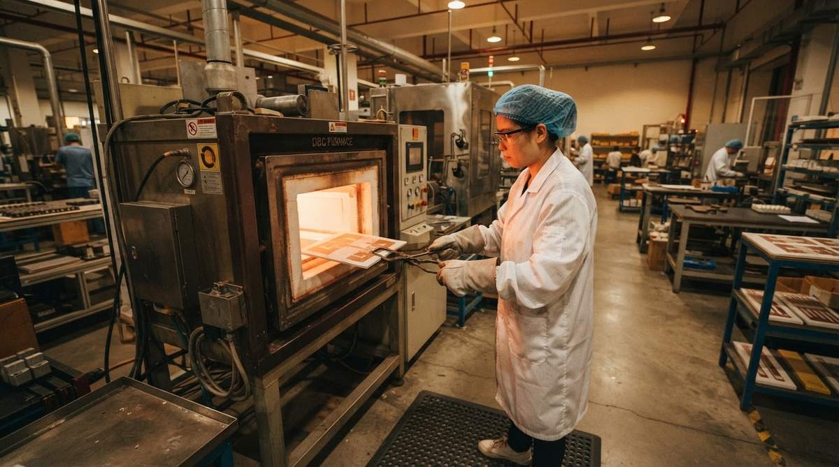
| DBC (Direct Bonded Copper) | 190 × 140 (common), up to 250 × 190 (specialty) | Furnace hot-zone uniformity |
| AMB (Active Metal Brazing) | 190 × 140 | Vacuum furnace capacity, braze uniformity |
| Thick Film (screen print) | 114 × 114 (typical), up to 152 × 152 | Screen frame size, paste uniformity |
| HTCC | Varies widely; green tape shrinkage limits practical size | Co-fire shrinkage control |
| LTCC | Up to ~150 × 150 (common) | Tape casting width, lamination press |
Ranges are representative of industry capability. Confirm with your manufacturer for the specific process line.
When a Larger Panel Is Not the Answer
If your individual board exceeds roughly 100 × 100 mm, ceramic may not be practical at all. Large single-piece ceramic boards are fragile, expensive to sinter with acceptable flatness, and hard to handle through automated assembly. Consider these alternatives:
- Metal-core PCB (MCPCB): Aluminum or copper core boards handle large areas well and cost far less, though thermal conductivity (1–4 W/mK for the dielectric layer) is much lower than bulk ceramic.
- FR-4 with embedded thermal vias: Adequate for moderate heat loads under ~2 W/cm² where ceramic’s 24–170 W/mK bulk conductivity is not required.
- Tiled ceramic on a metal baseplate: Multiple smaller ceramic substrates soldered or bonded to a common copper or AlSiC baseplate. Common in IGBT power modules.
For fast-turn evaluation of smaller designs, ceramic PCB prototyping services typically stock 114 × 114 mm blanks and can ship in days.
Design Tips for Panel Utilization
- Round your board outline to 0.5 mm increments. Odd dimensions waste scribe-street space.
- Orient the longest edge along the panel’s longest axis. This usually yields one or two extra rows.
- Combine multiple part numbers on one panel if volumes are low and both designs share the same substrate, thickness, and metallization stack. This is sometimes called “gang panelization.”
- Specify V-score over routing when possible. V-score streets are narrower (0.3 mm vs. 0.8–1.0 mm for routed tabs), recovering usable area.
Frequently Asked Questions
Can I get a ceramic PCB panel larger than 200 mm?
Rarely. Some DBC suppliers offer alumina panels up to approximately 250 × 190 mm, but availability is limited and per-panel cost is high. AlN and Si₃N₄ panels above 190 × 140 mm are uncommon in commercial production. For boards that large, a tiled approach on a metal baseplate is usually more reliable.
Does panel thickness affect the maximum available size?
Yes. Thinner substrates (0.25–0.38 mm) are harder to sinter flat at large sizes. A 190 × 140 mm panel is readily available at 0.635 mm thickness in Al₂O₃ 96%, but the same size at 0.25 mm may require tighter warpage screening or may not be offered at all.
How do I request a specific panel size from my supplier?
Start with the standard sizes your substrate vendor stocks. Custom sintered sizes require new tooling and minimum volumes—often 500+ blanks. If a standard size can be scribed to your needs, that is almost always faster and cheaper.
Is the panel size the same for DPC and DBC?
Not necessarily. DBC and AMB furnaces may accept different maximum panel dimensions than a DPC sputtering chamber. Always confirm the metallization process’s panel limit, not just the raw substrate size.
What is the minimum order for a full-panel run?
This varies by manufacturer and process. Prototype runs often start at 1–5 panels. Production MOQs may be 25–100 panels depending on the setup complexity. Ask for panel-level pricing, not just per-unit pricing, so you can evaluate yield economics directly.
Next Step
If you have a board outline and target material, send your Gerber files or a dimensioned drawing for a panel layout proposal and quote. The manufacturer can confirm which standard panel fits your design and how many units it yields. Understanding the ceramic substrate supply chain can also help you anticipate lead times for non-standard blank sizes.