Blog
-
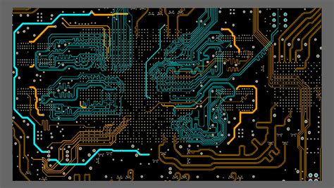
What is via covering in PCB?
Posted by
–
Read more: What is via covering in PCB?Introduction to Via covering Via covering is an essential technique used in the manufacturing of printed circuit boards (PCBs) to ensure the proper functioning and reliability of the board. In PCB Design, vias are small holes drilled through the board to create electrical connections between different layers. Via covering involves […]
-
 Read more: 3D Printer, Engraver and Etcher Combo – LumiPocket LT
Introduction to the LumiPocket LT The LumiPocket LT is a versatile and compact 3D printer, engraver, and etcher combo that offers a wide range of creative possibilities for hobbyists, designers, and professionals alike. This all-in-one device is designed to streamline your workflow and provide high-quality results in a user-friendly package. […]
-
About PCB Design Rules
Posted by
–
 Read more: About PCB Design Rules
Introduction to PCB Design Rules Printed Circuit Board (PCB) design is a complex process that involves creating an electronic circuit on a flat insulating substrate. PCB design rules are a set of guidelines and constraints that ensure the manufacturability, reliability, and functionality of the PCB. These rules are based on […]
-
PCB Silk-screen and Cure
Posted by
–
 Read more: PCB Silk-screen and Cure
What is PCB Silk-screen? PCB silk-screen, also known as legend or nomenclature, is the process of printing text, logos, or symbols onto the surface of a printed circuit board (PCB). This is typically done using a screen printing method, where ink is forced through a fine mesh screen onto the […]
-
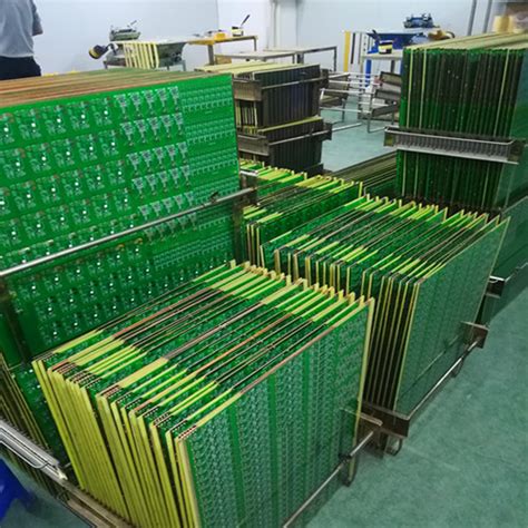
Tolerances on Printed Circuit Boards
Posted by
–
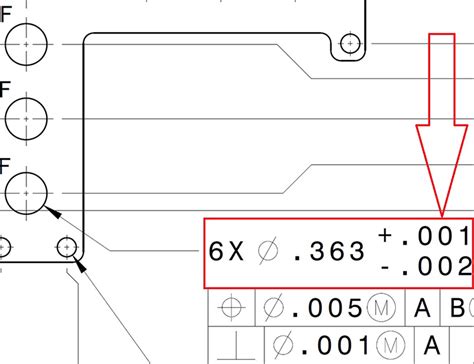 Read more: Tolerances on Printed Circuit Boards
Understanding PCB Tolerances and Their Importance Printed Circuit Boards (PCBs) are the backbone of modern electronic devices, connecting various components and ensuring proper functionality. To guarantee the reliability and performance of these devices, it is crucial to maintain strict tolerances during the PCB manufacturing process. In this comprehensive article, we […]
-
ACD Implements Altium Designer 10
Posted by
–
 Read more: ACD Implements Altium Designer 10
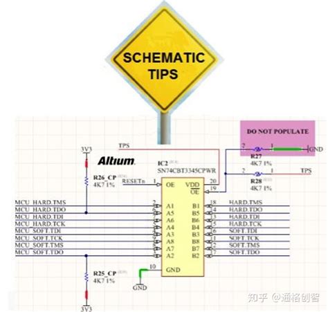
Introduction to ACD and Altium Designer ACD (Advanced Circuits Division) has recently implemented Altium Designer 10, a powerful electronic design automation (EDA) tool, to streamline its PCB design and manufacturing processes. This move is expected to significantly enhance ACD’s capabilities in delivering high-quality, innovative electronic solutions to its clients across […]
-
PCB Visualizer very much appreciated
Posted by
–
 Read more: PCB Visualizer very much appreciated
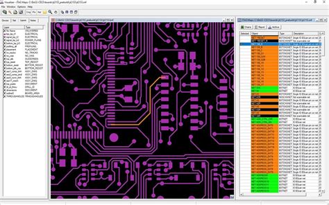
Introduction to PCB Visualizer PCB Visualizer is a powerful tool that allows engineers and designers to create, view, and analyze printed circuit board (PCB) designs in a 3D environment. It provides a realistic and interactive visualization of PCBs, enabling users to inspect the board layout, components, and connections from various […]
-
 Read more: A comparison of Multiple PCB design and EDA simulation tools
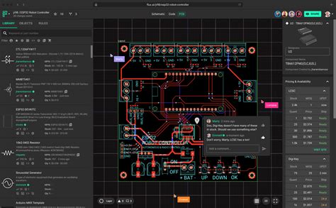
Introduction to PCB Design and EDA Simulation Tools Printed Circuit Board (PCB) design and Electronic Design Automation (EDA) simulation tools are essential for the development of modern electronic devices. These tools allow engineers to create, simulate, and optimize PCB layouts before the physical fabrication process begins. With the increasing complexity […]
-
Extend Extended Gerber – Gerber X2
Posted by
–
 Read more: Extend Extended Gerber – Gerber X2
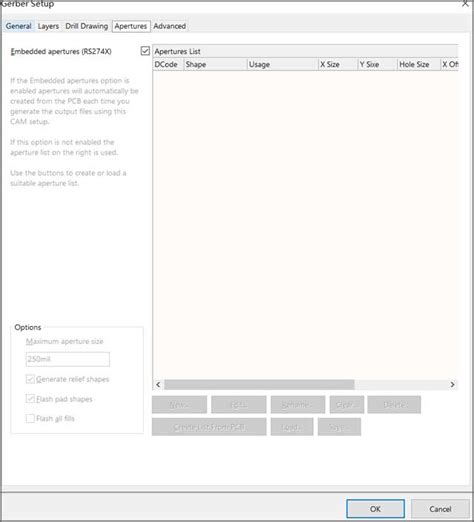
Introduction to Gerber X2 Gerber X2 is an extension of the Gerber file format, which is widely used in the PCB (printed circuit board) industry for transferring PCB design data. The original Extended Gerber format, also known as RS-274X, has been the de facto standard for PCB Fabrication data exchange […]
-
 Read more: Gerber File Ultimate Guide-A Beginner’s Guide to Gerber
What is a Gerber File? A Gerber file is a standard file format used in the electronic design automation (EDA) industry to describe the printed circuit board (PCB) images. It is a 2D binary vector image file format that was originally developed by the Gerber Systems Corp., a division of […]


