Blog
-
 Read more: Found A Place For Cheap Low Volume PCB Fabrication
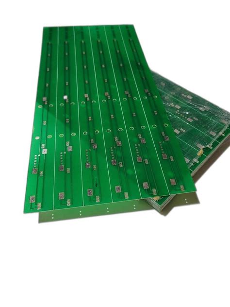
What is Low Volume PCB Fabrication? Low volume PCB fabrication refers to the production of printed circuit boards in small quantities, typically less than 1000 pieces. This is ideal for prototyping, small production runs, or custom projects where large quantities are not required. Request Alumina PCB Manufacturing Quote Now Why […]
-
How To Make The Etching PCBs
Posted by
–
 Read more: How To Make The Etching PCBs
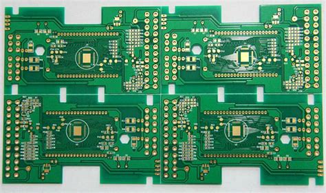
What is PCB Etching? PCB etching is the process of chemically removing unwanted copper from a printed circuit board (PCB) to create the desired electrical connections. It involves applying a resist layer to protect the copper traces that should remain, then submerging the PCB in an etchant solution to dissolve […]
-
6 Layer PCB Manufacturer With Stack up Types
Posted by
–
 Read more: 6 Layer PCB Manufacturer With Stack up Types
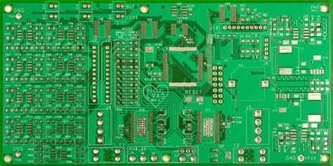
Introduction to PCB Stackups A printed circuit board (PCB) stackup refers to the arrangement of copper and insulating layers that make up a PCB. The stackup defines the number of layers, their order, thickness, and materials. Choosing the right PCB stackup is crucial for ensuring proper functionality, signal integrity, and […]
-
What is the PCB incoming inspection process?
Posted by
–
 Read more: What is the PCB incoming inspection process?
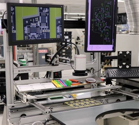
Why is PCB Incoming Inspection Important? PCB incoming inspection is a vital step in the electronics manufacturing process for several reasons: Identifying defects early: By inspecting PCBs upon arrival, manufacturers can identify any defects or issues before the boards are used in the assembly process. This early detection helps prevent […]
-
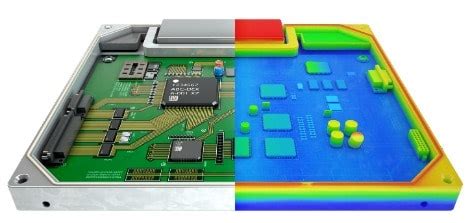 Read more: Digital Microscopes for Enhanced Inspection of Defects in Printed Circuit Boards
The Importance of PCB Inspection PCBs are the backbone of electronic devices, connecting and supporting various components to ensure proper functionality. However, during the manufacturing process, defects can occur due to a variety of factors, such as poor soldering, component misalignment, or contamination. These defects can lead to malfunctions, reduced […]
-
Copper PCB Manufacturers in China
Posted by
–
 Read more: Copper PCB Manufacturers in China
Why Choose Copper for PCBs? Copper is the most commonly used conductor material for PCBs due to its excellent electrical conductivity, thermal conductivity, and durability. Some key advantages of Copper PCBs include: High electrical conductivity enables efficient power transmission and signal integrity Good thermal conductivity helps dissipate heat for improved […]
-
 Read more: Methods For Final Quality Control In PCB Manufacturing
Visual Inspection Visual inspection is the most basic and common method for PCB Quality Control. Trained inspectors visually examine the PCBs for any obvious defects or irregularities. This process can be performed manually or with the assistance of automated optical inspection (AOI) systems. Manual Visual Inspection In manual visual inspection, […]
-
Mouse Bites PCB – Breakaway Tabs – V Groove PCB
Posted by
–
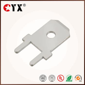 Read more: Mouse Bites PCB – Breakaway Tabs – V Groove PCB
Introduction to PCB Tabs and Mouse Bites Printed Circuit Boards (PCBs) are essential components in modern electronics, providing a platform for connecting and supporting various electronic components. In the manufacturing process of PCBs, it is common to produce multiple boards on a single panel to optimize production efficiency and reduce […]
-
X-Ray Inspection PCB Assembly Services in China
Posted by
–
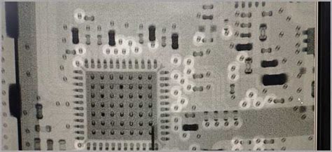 Read more: X-Ray Inspection PCB Assembly Services in China
Introduction to PCB X-Ray Inspection Printed Circuit Board (PCB) X-ray inspection is a non-destructive testing method used to inspect the internal structure of PCBs for defects or quality issues. It uses high-energy electromagnetic radiation to penetrate through the PCB and produce an image of its internal structure on a detector. […]
-
What Are Multi-layer Boards?
Posted by
–
 Read more: What Are Multi-layer Boards?
Introduction to Multi-layer Boards Multi-layer boards, also known as multi-layer printed circuit boards (PCBs), are essential components in modern electronic devices. These boards consist of multiple layers of conductive material, typically copper, separated by insulating layers. The conductive layers are interconnected through vias, which are small holes drilled through the […]


