Blog
-
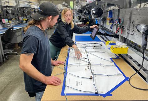
Read more: Wire Harness Manufacturing Process – A Step by Step Guide
What is a Wire Harness? A wire harness, also known as a cable harness or wiring loom, is an assembly of electrical wires or cables that transmit signals or electrical power. It is designed to simplify the wiring system by bundling multiple wires together, providing a more organized and efficient […]
-
Custom Wire Harness Manufacturer
Posted by
–
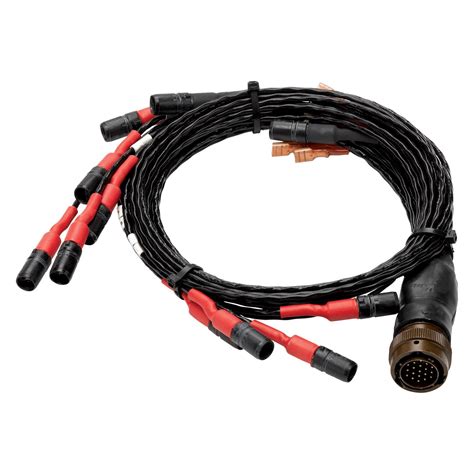
 Read more: Custom Wire Harness Manufacturer
What is a Wire Harness? A wire harness is a collection of wires, cables, connectors, and terminals that are pre-assembled into a single unit to simplify the installation and interconnection of electrical components. The purpose of a wire harness is to efficiently and securely transmit electrical signals or power between […]
-
Cable & Wire Harness Assembly
Posted by
–
 Read more: Cable & Wire Harness Assembly
What is a Wire Harness? A wire harness, also known as a cable harness or wiring loom, is a systematic and organized assembly of electrical wires, cables, and connectors that are designed to transmit signals or electrical power throughout a vehicle, machine, or electronic device. The primary purpose of a […]
-
ELECTRONICS CONTRACT MANUFACTURER
Posted by
–
 Read more: ELECTRONICS CONTRACT MANUFACTURER
What is an Electronics Contract Manufacturer (ECM)? An Electronics Contract Manufacturer (ECM) is a company that specializes in the design, development, and production of electronic components and assemblies for other companies. ECMs provide a wide range of services, including printed circuit board (PCB) assembly, cable and wire harness assembly, box […]
-
The Common Gold Plating Process for PCBs
Posted by
–
 Read more: The Common Gold Plating Process for PCBs
What is Gold Plating? Gold plating is an electroplating process that involves depositing a thin layer of gold onto the surface of a PCB. The gold layer is typically applied over a nickel underlayer, which serves as a barrier between the copper substrate and the gold layer. The nickel layer […]
-
Active & Passive Components
Posted by
–
 Read more: Active & Passive Components
What are Active and Passive Components in Electronics? Electronic circuits are made up of various components that can be broadly classified into two categories: active components and passive components. Understanding the difference between these two types of components is crucial for anyone working with electronic circuits. Active Components Active components […]
-
 Read more: Electronic Collaborative Manufacturing Service System (ECMS)
What is ECMS? An Electronic Collaborative Manufacturing Service System (ECMS) is an integrated platform that enables companies to collaborate electronically throughout the entire manufacturing process, from design and development to production and delivery. ECMS solutions leverage advanced technologies like cloud computing, Internet of Things (IoT), artificial intelligence (AI), and big […]
-
 Read more: IPC-A-600 Acceptability of Printed Boards: Classes
What is IPC-A-600? IPC-A-600 is a widely recognized standard published by the Association Connecting Electronics Industries (IPC) that provides acceptance criteria for printed circuit boards (PCBs). This standard is essential for ensuring the quality and reliability of PCBs used in various electronic applications. It defines the acceptable conditions of boards […]
-
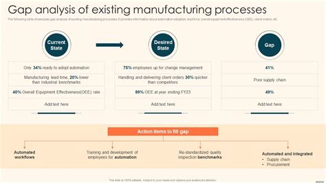 Read more: The difference between Production and Prototype quality and how to bridge the gap?
Understanding the Production-Prototype Gap In the world of manufacturing and product development, there exists a significant gap between prototype quality and production quality. This gap, known as the “Production-Prototype Gap,” can lead to numerous challenges and setbacks for companies striving to bring their innovative ideas to market. Understanding the differences […]
-
Selecting the Right Surface Finish for your PCB
Posted by
–
 Read more: Selecting the Right Surface Finish for your PCB
Understanding Surface Finish and its Importance in PCB Manufacturing When designing and manufacturing printed circuit boards (PCBs), one crucial aspect to consider is the surface finish. The surface finish is the coating applied to the exposed copper on the PCB, which serves multiple purposes, such as protecting the copper from […]


