What are Bypass and Decoupling Capacitors?
Bypass capacitors and decoupling capacitors are two types of capacitors commonly used in electronic circuits to help reduce noise and stabilize power supply voltages. While they serve similar purposes, there are some key differences between bypass and decoupling capacitors in terms of their placement, values, and specific functions. Understanding these differences is important for properly designing circuits and optimizing performance.
Key Differences Between Bypass and Decoupling Capacitors
| Property | Bypass Capacitor | Decoupling Capacitor |
|---|---|---|
| Placement | Physically close to IC power pins | Distributed across power planes |
| Capacitance Value | Smaller (nF range) | Larger (uF range) |
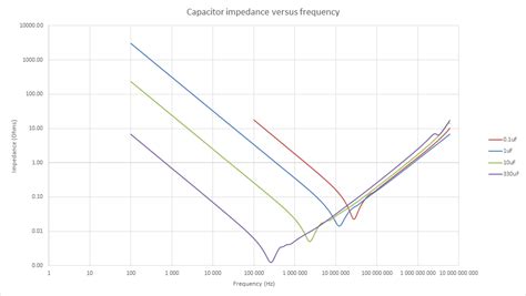
| Frequency Response | Effective at higher frequencies | Effective at lower frequencies |
| Main Purpose | Shunt high-frequency noise | Smooth low-frequency voltage ripple |
How Bypass Capacitors Work
A bypass capacitor, also known as a local decoupling capacitor, is a small capacitor placed in very close proximity to the power supply pins of an integrated circuit (IC). Its main purpose is to provide a low-impedance path to ground for high-frequency noise that may be present on the power supply lines. By “bypassing” or “shorting out” this noise, the bypass capacitor helps maintain a clean and stable supply voltage for the IC.
Selecting the Right Bypass Capacitor Value
The value of a bypass capacitor is typically in the nanofarad (nF) range, with common values being 0.1uF (100nF), 0.01uF (10nF), and 0.001uF (1nF). The specific value chosen depends on factors such as the IC’s power requirements, the expected noise frequencies, and the PCB layout.
As a general rule of thumb, the capacitance value should be large enough to provide a low impedance path at the frequencies of concern, but not so large that it becomes ineffective at higher frequencies. The reactance of a capacitor decreases with increasing frequency, so smaller capacitors are more effective at bypassing high-frequency noise.
Bypass Capacitor Placement and Layout
Proper placement of bypass capacitors is crucial for their effectiveness. They should be located as close as possible to the IC power pins to minimize the inductance of the connecting traces. Inductance limits the capacitor’s ability to respond quickly to sudden changes in current demand, reducing its effectiveness at high frequencies.
Ideally, bypass capacitors should be connected directly to the IC power and ground pins using short, wide traces or power planes. This minimizes the loop area and reduces the inductance of the connection. In some cases, it may be necessary to use multiple bypass capacitors in parallel to further reduce the effective inductance and provide a cleaner supply voltage.

How Decoupling Capacitors Work
Decoupling capacitors, also known as bulk capacitors or reservoir capacitors, serve a similar purpose to bypass capacitors but at a larger scale. They are typically placed across the power supply rails of a circuit board to help smooth out low-frequency voltage fluctuations and provide a stable supply voltage to the entire circuit.
Decoupling Capacitor Values and Selection
Decoupling capacitors are usually larger than bypass capacitors, with values in the microfarad (uF) range. Common values include 10uF, 22uF, and 47uF, although the specific value used depends on the power requirements of the circuit and the expected voltage fluctuations.
The main factors to consider when selecting a decoupling capacitor are its capacitance value, voltage rating, and equivalent series resistance (ESR). The capacitance value should be large enough to provide sufficient energy storage and smoothing of voltage ripple, while the voltage rating must exceed the maximum expected voltage on the power rail. Low ESR is desirable to minimize power loss and heating of the capacitor.
Decoupling Capacitor Placement and Layout
Unlike bypass capacitors, which are placed close to individual ICs, decoupling capacitors are distributed across the power planes of a circuit board. They are typically located near the power supply input and at strategic points along the power distribution network to minimize impedance and ensure a stable supply voltage throughout the circuit.
Proper layout techniques for decoupling capacitors include using wide, low-impedance power and ground planes, minimizing the loop area between the capacitor and the power planes, and using multiple capacitors in parallel to reduce the effective ESR and inductance. It’s also important to consider the frequency response of the decoupling capacitors and choose values that are effective at the frequencies of interest.

Combining Bypass and Decoupling Capacitors
While bypass and decoupling capacitors serve different purposes and are placed differently on a circuit board, they work together to provide a complete power supply filtering solution. Decoupling capacitors smooth out low-frequency voltage fluctuations and provide a stable voltage to the entire circuit, while bypass capacitors filter high-frequency noise at individual ICs.
A typical power supply filtering network consists of one or more large decoupling capacitors near the power input, smaller decoupling capacitors distributed throughout the power planes, and tiny bypass capacitors at each IC. This hierarchical approach ensures that noise and voltage fluctuations are filtered effectively across a wide frequency range.
Selecting the Right Combination of Capacitors
Choosing the right combination of bypass and decoupling capacitors depends on the specific requirements of the circuit, including the expected noise frequencies, power consumption, and layout constraints. As a starting point, designers often use standard values such as 0.1uF for bypass capacitors and 10uF for decoupling capacitors, then adjust these values based on simulation results and real-world measurements.
It’s also important to consider the frequency response of the capacitors and ensure that there is adequate filtering across the entire frequency range of interest. This may require using multiple capacitors with different values in parallel to achieve the desired response.
Layout Considerations for Combined Filtering
When laying out a combined bypass and decoupling capacitor network, it’s important to follow best practices for each type of capacitor. This includes placing bypass capacitors as close as possible to IC power pins, using wide and low-impedance power planes for decoupling capacitors, and minimizing loop areas and trace inductances.
It’s also important to consider the interactions between bypass and decoupling capacitors and ensure that they don’t interfere with each other. For example, placing a large decoupling capacitor too close to a bypass capacitor can reduce the effectiveness of the bypass capacitor at high frequencies due to the added inductance of the decoupling capacitor’s leads.

Simulation and Measurement Techniques
To ensure that a power supply filtering network is effective, it’s important to simulate the circuit’s behavior and measure its performance in the real world. Simulation tools such as SPICE can be used to model the frequency response of the capacitors and predict the noise levels at various points in the circuit.
Real-world measurements can be made using oscilloscopes, spectrum analyzers, and network analyzers to verify that the filtering network is performing as expected. Techniques such as impedance spectroscopy and noise injection can be used to characterize the frequency response of the capacitors and identify any potential issues.
Interpreting Simulation and Measurement Results
When interpreting simulation and measurement results, it’s important to look for key indicators of a well-designed filtering network. These include:
- Low impedance across the frequency range of interest
- Smooth and stable power supply voltages at all ICs
- Minimal noise and ripple on the power rails
- Consistent performance across temperature and voltage variations
If any of these indicators are not met, it may be necessary to adjust the capacitor values, placement, or layout to improve the filtering performance.
Examples and Case Studies
To illustrate the concepts discussed in this article, let’s look at a few examples and case studies of bypass and decoupling capacitor usage in real-world circuits.
Example 1: Simple Microcontroller Circuit
Consider a simple microcontroller circuit powered by a 5V supply. The microcontroller has a single power pin and a ground pin, and the circuit includes a 0.1uF bypass capacitor placed close to the power pin.
In this case, the bypass capacitor helps to filter out high-frequency noise that may be present on the power supply line, ensuring a clean and stable voltage for the microcontroller. The 0.1uF value is chosen as a standard value that provides good high-frequency performance without being too large to place close to the IC.
Example 2: Complex Digital Circuit
Now consider a more complex digital circuit with multiple ICs and power rails. The circuit includes several large decoupling capacitors (e.g., 10uF and 22uF) placed near the power supply input and smaller decoupling capacitors (e.g., 1uF) distributed throughout the power planes. Each IC has its own 0.1uF bypass capacitor placed close to its power pins.
In this case, the large decoupling capacitors help to smooth out low-frequency voltage fluctuations and provide a stable voltage to the entire circuit. The smaller decoupling capacitors help to reduce impedance and maintain a stable voltage at different points along the power distribution network. The bypass capacitors filter out high-frequency noise at each IC, ensuring a clean and stable supply voltage for each device.
Case Study: Debugging a Noisy Power Supply
In this case study, an engineer is debugging a circuit that experiences intermittent failures and glitches. Oscilloscope measurements reveal significant noise and voltage fluctuations on the power supply rails, indicating a problem with the power supply filtering network.
To troubleshoot the issue, the engineer first checks the placement and values of the decoupling and bypass capacitors. They discover that some of the bypass capacitors are placed too far from their respective ICs, reducing their effectiveness at high frequencies. Additionally, the decoupling capacitors are found to be undersized for the circuit’s power requirements.
To fix the problem, the engineer makes several changes to the filtering network:
- Larger decoupling capacitors are added near the power supply input to improve low-frequency filtering
- Additional decoupling capacitors are placed along the power distribution network to reduce impedance and voltage fluctuations
- Bypass capacitors are moved closer to their respective ICs and connected with shorter, wider traces to minimize inductance
After making these changes, the engineer re-tests the circuit and finds that the noise and voltage fluctuations have been significantly reduced, and the intermittent failures have been eliminated. This case study illustrates the importance of proper component selection and placement in power supply filtering networks.
FAQ
1. What is the difference between a bypass capacitor and a decoupling capacitor?
Bypass capacitors and decoupling capacitors are both used to filter noise and stabilize voltage in electronic circuits, but they differ in their placement, values, and specific functions. Bypass capacitors are small (typically in the nF range) and placed very close to IC power pins to filter high-frequency noise. Decoupling capacitors are larger (typically in the uF range) and distributed across power planes to smooth out low-frequency voltage fluctuations and provide a stable voltage to the entire circuit.
2. How do I select the right capacitor values for my circuit?
Selecting the right capacitor values depends on the specific requirements of your circuit, including the expected noise frequencies, power consumption, and layout constraints. As a starting point, designers often use standard values such as 0.1uF for bypass capacitors and 10uF for decoupling capacitors, then adjust these values based on simulation results and real-world measurements. It’s also important to consider the frequency response of the capacitors and ensure that there is adequate filtering across the entire frequency range of interest.
3. What are some common layout techniques for bypass and decoupling capacitors?
Proper layout is crucial for the effectiveness of bypass and decoupling capacitors. For bypass capacitors, place them as close as possible to the IC power pins and connect them with short, wide traces or power planes to minimize inductance. For decoupling capacitors, distribute them across the power planes and use wide, low-impedance traces to minimize impedance. In both cases, minimize loop areas and consider the interactions between capacitors to avoid interference.
4. How can I test the effectiveness of my power supply filtering network?
To test the effectiveness of your power supply filtering network, use a combination of simulation tools (such as SPICE) and real-world measurements (using oscilloscopes, spectrum analyzers, and network analyzers). Look for key indicators such as low impedance across the frequency range of interest, smooth and stable power supply voltages at all ICs, minimal noise and ripple on the power rails, and consistent performance across temperature and voltage variations. If any issues are identified, adjust the capacitor values, placement, or layout as needed.
5. Can I use just one type of capacitor (bypass or decoupling) in my circuit?
While it is possible to use just one type of capacitor in a circuit, using a combination of bypass and decoupling capacitors is generally recommended for optimal power supply filtering. Decoupling capacitors smooth out low-frequency voltage fluctuations and provide a stable voltage to the entire circuit, while bypass capacitors filter high-frequency noise at individual ICs. By using both types of capacitors in a hierarchical approach, you can ensure effective noise filtering across a wide frequency range.
Conclusion
In conclusion, understanding the difference between bypass and decoupling capacitors is crucial for designing effective power supply filtering networks in electronic circuits. Bypass capacitors are small, placed close to IC power pins, and filter high-frequency noise, while decoupling capacitors are larger, distributed across power planes, and smooth out low-frequency voltage fluctuations.
By selecting the right capacitor values, placing them properly on the circuit board, and using a combination of both types of capacitors, designers can ensure a clean and stable power supply for their circuits. Simulation tools and real-world measurements can help verify the effectiveness of the filtering network and identify any potential issues.
As electronic circuits continue to become more complex and operate at higher frequencies, the importance of effective power supply filtering will only continue to grow. By mastering the concepts of bypass and decoupling capacitors, designers can create robust and reliable circuits that perform well in even the most demanding applications.


Leave a Reply