What is PCB Copper Balance and Why is it Important?
PCB copper balance refers to the even distribution of copper on both sides of a printed circuit board (PCB) during the fabrication process. Maintaining proper copper balance is critical for several reasons:
- Preventing warping and twisting of the PCB
- Ensuring consistent electrical properties
- Improving the reliability and longevity of the PCB
- Facilitating proper etching and plating processes
When copper is unevenly distributed on a PCB, it can lead to a variety of issues that impact the board’s performance and reliability. Unbalanced copper can cause the PCB to warp or twist during the fabrication process, which can result in misaligned components, poor soldering, and even cracking of the board.
Furthermore, uneven copper distribution can affect the electrical properties of the PCB. Copper thickness variations can lead to inconsistent impedance, signal integrity issues, and increased electromagnetic interference (EMI).
Factors Affecting PCB Copper Balance
Several factors can influence the copper balance on a PCB during fabrication:
PCB Design
The design of the PCB plays a significant role in maintaining copper balance. Some key design considerations include:
- Symmetrical layout: A symmetrical layout helps ensure even copper distribution on both sides of the board.
- Balanced copper pour: Copper pour should be evenly distributed across the PCB to avoid areas with excessive or insufficient copper.
- Proper trace width and spacing: Consistent trace widths and spacing help maintain copper balance and minimize the risk of Etching Issues.
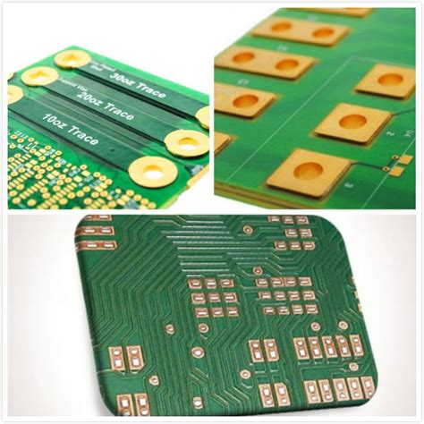
Copper Foil Thickness
The thickness of the copper foil used in PCB fabrication can also impact copper balance. Standard copper foil thicknesses for PCBs include:
| Copper Weight (oz) | Thickness (μm) |
|---|---|
| 0.5 | 17.5 |
| 1 | 35 |
| 2 | 70 |
| 3 | 105 |
Using consistent copper foil thickness throughout the PCB helps maintain copper balance. Mixing different thicknesses can lead to uneven distribution and potential issues during fabrication.
Etching Process
The etching process, which removes unwanted copper from the PCB, can significantly affect copper balance. Factors to consider include:
- Etchant concentration: Proper etchant concentration ensures consistent copper removal across the board.
- Etching time: Excessive etching time can lead to over-etching, resulting in uneven copper distribution.
- Etching uniformity: Uneven etching can cause localized areas of excessive or insufficient copper removal.
Plating Process
The plating process, which deposits additional copper onto the PCB, can also impact copper balance. Key factors include:
- Plating thickness: Consistent plating thickness helps maintain copper balance across the board.
- Plating uniformity: Uneven plating can lead to localized areas of excessive or insufficient copper deposition.

Techniques for Maintaining PCB Copper Balance
To maintain proper copper balance during PCB fabrication, several techniques can be employed:
Design for Manufacturing (DFM)
Incorporating DFM principles into the PCB design process can help ensure copper balance. Some DFM guidelines include:
- Symmetrical layout: Designing the PCB with a symmetrical layout helps distribute copper evenly on both sides of the board.
- Balanced copper distribution: Ensuring that copper is evenly distributed across the PCB, avoiding large areas of continuous copper or isolated traces.
- Consistent trace width and spacing: Maintaining consistent trace widths and spacing throughout the design helps ensure even copper distribution and minimize etching issues.
Copper Thieving
Copper thieving is a technique used to balance copper distribution on a PCB. It involves adding non-functional copper areas, known as “thieving pads,” to regions of the board with insufficient copper. These pads help distribute copper more evenly during the etching and plating processes.
Copper thieving pads should be strategically placed in areas with minimal copper, such as large ground planes or isolated traces. The size and shape of the thieving pads can vary depending on the specific design requirements and the amount of copper balancing needed.
Panelization
Panelization is the process of grouping multiple PCBs onto a single panel for fabrication. Proper panelization can help maintain copper balance by ensuring that the copper distribution is consistent across the entire panel.
When panelizing PCBs, it’s important to consider the following:
- Panel layout: Arranging the PCBs on the panel in a symmetrical and balanced manner helps distribute copper evenly.
- Panel borders: Including sufficient border space around the individual PCBs allows for even copper distribution during etching and plating.
- Tooling holes: Placing tooling holes strategically on the panel helps ensure consistent alignment and copper distribution during fabrication.
Process Control
Maintaining strict process control during PCB fabrication is crucial for achieving proper copper balance. This involves:
- Etchant concentration monitoring: Regularly monitoring and adjusting the etchant concentration ensures consistent copper removal across the board.
- Etching time control: Carefully controlling the etching time prevents over-etching and ensures even copper distribution.
- Plating thickness monitoring: Regularly measuring and adjusting the plating thickness helps maintain consistent copper deposition across the board.

Measuring and Verifying PCB Copper Balance
To ensure that proper copper balance has been achieved, several measurement and verification techniques can be employed:
Visual Inspection
A visual inspection of the PCB can provide an initial assessment of copper balance. Look for signs of uneven copper distribution, such as:
- Warping or twisting of the board
- Inconsistent trace widths or spacing
- Localized areas of excessive or insufficient copper
Resistance Measurements
Measuring the resistance of copper traces on both sides of the PCB can help verify copper balance. Consistent resistance values across the board indicate even copper distribution.
X-Ray Fluorescence (XRF) Analysis
XRF analysis is a non-destructive technique that measures the thickness and composition of copper on a PCB. By comparing XRF measurements from different areas of the board, copper balance can be assessed.
Cross-Sectional Analysis
Cross-sectional analysis involves cutting a small section of the PCB and examining it under a microscope. This destructive technique allows for a detailed view of the copper distribution and can help identify any localized issues.

FAQ
1. What is the ideal copper balance for a PCB?
The ideal copper balance for a PCB depends on the specific design requirements and the intended application. Generally, a copper balance within ±10% is considered acceptable for most PCBs. However, more stringent requirements may apply for high-frequency or high-reliability applications.
2. Can copper imbalance cause signal integrity issues?
Yes, copper imbalance can cause signal integrity issues. Uneven copper distribution can lead to inconsistent impedance, increased crosstalk, and signal reflections. These issues can be particularly problematic for high-speed digital circuits and high-frequency analog signals.
3. How does the PCB material affect copper balance?
The choice of PCB material can impact copper balance. Different materials have varying thermal expansion coefficients, which can cause uneven copper distribution during the fabrication process. It’s important to select a PCB material that is compatible with the desired copper balance and the specific application requirements.
4. Can copper balance issues be corrected after PCB fabrication?
In most cases, copper balance issues cannot be easily corrected after PCB fabrication. While some localized issues may be addressed through selective plating or etching, significant copper imbalances often require a redesign and refabrication of the PCB.
5. How can I ensure copper balance when outsourcing PCB fabrication?
When outsourcing PCB fabrication, it’s important to work with a reputable and experienced manufacturer. Provide clear specifications for copper balance requirements and discuss any specific design considerations with the manufacturer. Request regular updates and inspection reports throughout the fabrication process to ensure that copper balance is being maintained.
Conclusion
Maintaining proper copper balance is essential for ensuring the reliability, performance, and longevity of printed circuit boards. By understanding the factors that affect copper balance and employing appropriate design and fabrication techniques, PCB manufacturers can consistently produce high-quality boards that meet the desired specifications.
Effective communication between PCB designers and fabricators is crucial for achieving optimal copper balance. By working together to address copper balance considerations throughout the design and fabrication process, teams can minimize the risk of issues and ensure the successful production of reliable and high-performing PCBs.


Leave a Reply