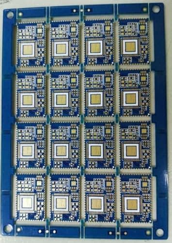
What is PCB cloning?
PCB cloning is the process of creating an exact replica of an existing PCB. This involves analyzing the original board, extracting the design information, and reproducing it on a new PCB. The goal is to create a functionally identical copy of the original board, maintaining its electrical and mechanical properties.
Why Clone PCBs?
There are several reasons why PCB cloning is essential in the electronics industry:
-
Reverse Engineering: PCB cloning allows engineers to study and understand the design of an existing board. By analyzing the cloned PCB, they can learn about the circuit design, component selection, and layout techniques used in the original board.
-
Obsolescence Management: When a particular PCB becomes obsolete or is no longer available from the original manufacturer, cloning provides a way to reproduce the board and ensure continuity of production.
-
Cost Reduction: Cloning an existing PCB can be more cost-effective than designing a new board from scratch. It eliminates the need for extensive design and testing efforts, reducing development time and costs.
-
Customization: PCB cloning allows for modifications and improvements to be made to an existing design. Engineers can clone a board and incorporate changes to enhance its functionality or adapt it to specific requirements.
PCB Cloning Techniques
There are several techniques used for PCB cloning, depending on the available resources and the complexity of the original board. Let’s explore some of the common methods:
Visual Inspection and Manual Tracing
The most basic approach to PCB cloning is through visual inspection and manual tracing. This method involves examining the original board closely, identifying components, and manually tracing the connections between them. The traced information is then used to create a schematic diagram and PCB layout.
While this method can be effective for simple boards, it becomes increasingly challenging and time-consuming as the complexity of the board increases. It also relies heavily on the skill and experience of the person performing the cloning.
X-Ray Imaging
X-ray imaging is a non-destructive technique used to analyze the internal structure of a PCB. By capturing X-ray images of the board from different angles, engineers can visualize the layers, traces, and vias within the PCB.
X-ray imaging provides a detailed view of the board’s construction, enabling accurate reconstruction of the PCB design. However, this method requires specialized equipment and expertise to interpret the X-ray images effectively.
3D Scanning
3D scanning is an advanced technique that utilizes specialized scanners to create a three-dimensional digital model of the PCB. The scanner captures the surface geometry, component placement, and trace routing of the board.
The resulting 3D model can be used to generate a detailed PCB layout and schematic diagram. 3D scanning offers high accuracy and efficiency in PCB cloning, especially for complex boards with intricate designs.
Desoldering and Reverse Engineering
In some cases, PCB cloning may involve desoldering components from the original board to gain access to the underlying traces and connections. This destructive approach allows for direct examination of the board’s internal structure.
Once the components are removed, the exposed traces can be traced and documented to recreate the PCB design. This method is typically used when non-destructive techniques are not feasible or when a complete understanding of the board’s functionality is required.

Best Practices for PCB Cloning
To ensure successful PCB cloning, consider the following best practices:
-
Documentation: Maintain thorough documentation throughout the cloning process. Record the component values, trace routing, and any specific notes or observations. This documentation will serve as a valuable reference during the reproduction phase.
-
Component Sourcing: Identify and source the exact components used in the original board. If the exact components are not available, find suitable replacements with equivalent specifications and footprints.
-
Design Verification: Verify the cloned PCB design against the original board. Compare the schematic diagram, component placement, and trace routing to ensure accuracy and compatibility.
-
Prototype Testing: Fabricate a prototype of the cloned PCB and thoroughly test its functionality. Perform electrical tests, signal integrity checks, and any application-specific tests to validate the cloned board’s performance.
-
Compliance and Regulations: Ensure that the cloned PCB complies with relevant industry standards and regulations. Consider factors such as electromagnetic compatibility (EMC), safety requirements, and environmental regulations.

Challenges in PCB Cloning
While PCB cloning offers numerous benefits, it also presents several challenges that need to be addressed:
Intellectual Property (IP) Concerns
PCB cloning may raise intellectual property concerns, especially if the original board is protected by patents or copyrights. It is crucial to ensure that the cloning process does not infringe upon any existing IP rights. Obtain necessary permissions or licenses before proceeding with cloning.
Component Obsolescence
One of the challenges in PCB cloning is dealing with obsolete components. If the original board uses components that are no longer available, finding suitable replacements can be difficult. It may require extensive research and testing to identify compatible alternatives.
Design Complexity
As PCB designs become more complex, with high-density layouts and advanced manufacturing techniques, cloning becomes increasingly challenging. Multilayer boards, fine-pitch components, and specialized materials can complicate the cloning process, requiring advanced tools and expertise.
Manufacturing Considerations
When cloning a PCB, it is essential to consider the manufacturing capabilities and limitations. The cloned board should be designed to meet the manufacturing requirements, such as minimum trace widths, pad sizes, and via specifications. Collaboration with the manufacturing facility is crucial to ensure successful fabrication.

Frequently Asked Questions (FAQ)
-
Is PCB cloning legal?
PCB cloning is legal as long as it does not infringe upon any intellectual property rights. It is essential to obtain necessary permissions or licenses before cloning a protected board. -
How accurate is PCB cloning?
The accuracy of PCB cloning depends on the techniques used and the complexity of the original board. Advanced methods like 3D scanning and X-ray imaging offer high accuracy, while manual tracing may introduce some discrepancies. -
Can PCB cloning be used for commercial purposes?
PCB cloning can be used for commercial purposes, provided that it complies with legal and ethical guidelines. It is important to respect intellectual property rights and obtain necessary permissions before commercializing a cloned board. -
What tools are required for PCB cloning?
The tools required for PCB cloning vary depending on the techniques used. Common tools include schematic capture software, PCB layout software, X-ray imaging equipment, 3D scanners, and soldering/desoldering tools. -
How long does PCB cloning take?
The duration of PCB cloning depends on the complexity of the board and the techniques employed. Simple boards using manual tracing may take a few days, while complex boards requiring advanced techniques like 3D scanning can take several weeks.
Conclusion
PCB cloning is a valuable technique in the electronics industry, enabling reverse engineering, obsolescence management, cost reduction, and customization. By understanding the various techniques, best practices, and challenges associated with PCB cloning, engineers and manufacturers can leverage this process effectively.
However, it is crucial to approach PCB cloning with legal and ethical considerations in mind. Respecting intellectual property rights and obtaining necessary permissions are essential to ensure compliance and maintain the integrity of the cloning process.
As technology advances and PCB designs become more complex, PCB cloning techniques will continue to evolve. Staying updated with the latest tools, techniques, and best practices is key to successful PCB cloning in the ever-changing landscape of electronics manufacturing.
| Technique | Advantages | Disadvantages |
|---|---|---|
| Visual Inspection and Manual Tracing | – Low cost – Suitable for simple boards |
– Time-consuming – Relies on human skill and accuracy |
| X-Ray Imaging | – Non-destructive – Provides detailed internal view |
– Requires specialized equipment – Expertise needed for interpretation |
| 3D Scanning | – High accuracy – Efficient for complex boards |
– Expensive equipment – Requires specialized software |
| Desoldering and Reverse Engineering | – Direct examination of internal structure – Enables complete understanding of functionality |
– Destructive approach – Time-consuming and labor-intensive |
By combining the appropriate techniques, following best practices, and addressing the challenges, PCB cloning can be a powerful tool for electronics professionals to replicate, analyze, and improve existing PCB designs.


Leave a Reply