Introduction to PCB cloning
PCB (Printed Circuit Board) cloning is the process of creating an exact replica of an existing PCB design. This technique is used when the original PCB design files are not available, or when a physical board needs to be reverse-engineered. PCB cloning is a valuable tool for electronics enthusiasts, hobbyists, and professionals who need to reproduce or modify existing PCB designs.
What is a Printed Circuit Board (PCB)?
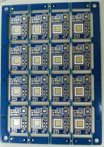
A Printed Circuit Board (PCB) is a flat board made of insulating material, such as fiberglass or plastic, with conductive tracks, pads, and other features etched or printed on its surface. PCBs are used to mechanically support and electrically connect electronic components using conductive pathways, tracks, or signal traces.
| PCB Type | Description |
|---|---|
| Single-sided | Components are mounted on one side of the board, with conductive tracks on the opposite side. |
| Double-sided | Components and conductive tracks are present on both sides of the board. |
| Multi-layer | Multiple layers of conductive tracks are sandwiched between insulating layers, allowing for more complex designs and higher component density. |
The PCB Cloning Process
The PCB cloning process involves several steps to accurately reproduce an existing PCB design. These steps include:
1. PCB Imaging
The first step in PCB cloning is to capture high-quality images of the original PCB. This can be done using a flatbed scanner or a high-resolution digital camera. It is essential to capture clear images of both sides of the PCB, ensuring that all components, tracks, and markings are visible.
2. Image Processing
Once the PCB images are captured, they need to be processed to enhance their clarity and remove any distortions or artifacts. Image processing software, such as Adobe Photoshop or GIMP, can be used to adjust the brightness, contrast, and color balance of the images. The goal is to create a clear and accurate representation of the original PCB.
3. PCB Layout Reconstruction
With the processed images, the next step is to reconstruct the PCB layout using PCB design software, such as KiCad, Eagle, or Altium Designer. This involves tracing the conductive tracks, placing components, and adding any necessary markings or labels. The reconstructed PCB layout should be an exact replica of the original design.
4. Component Identification
To complete the PCB cloning process, it is necessary to identify the components used on the original board. This can be done by visually inspecting the components and comparing them to datasheets or component libraries. In some cases, it may be necessary to desolder components from the original board to determine their values or part numbers.
5. PCB Fabrication
Once the PCB layout is reconstructed and the components are identified, the cloned PCB can be fabricated using standard PCB manufacturing techniques. This involves generating Gerber files from the PCB design software and sending them to a PCB manufacturer for production.

Advantages of PCB Cloning
PCB cloning offers several advantages for electronics enthusiasts, hobbyists, and professionals:
-
Reverse Engineering: PCB cloning allows for the reverse engineering of existing PCB designs when the original design files are not available. This is particularly useful for repairing or modifying older electronic devices or for learning from existing designs.
-
Design Modification: By cloning an existing PCB, designers can easily modify the design to suit their specific needs. This can include adding or removing components, changing the board layout, or optimizing the design for better performance.
-
Cost Savings: PCB cloning can be a cost-effective alternative to designing a PCB from scratch, especially for simple or small-scale projects. By starting with an existing design, designers can save time and resources that would otherwise be spent on the design process.
-
Educational Value: PCB cloning is an excellent way for students and hobbyists to learn about PCB design and electronics. By studying and replicating existing designs, learners can gain valuable insights into the design process and develop their skills in PCB layout and component selection.

Challenges and Limitations of PCB Cloning
While PCB cloning offers many benefits, there are also some challenges and limitations to consider:
-
Image Quality: The success of PCB cloning heavily depends on the quality of the captured images. Poor image quality can lead to inaccuracies in the reconstructed PCB layout, resulting in a non-functional or suboptimal cloned board.
-
Component Identification: Identifying components can be challenging, especially for older or obscure parts. In some cases, it may be necessary to desolder components from the original board to determine their values or part numbers, which can be time-consuming and potentially damaging to the components.
-
Legal Considerations: PCB cloning may raise legal concerns, particularly if the original PCB design is protected by intellectual property rights, such as patents or copyrights. It is essential to ensure that any cloning activities comply with applicable laws and regulations.
-
Design Complexity: Complex PCB designs, such as those with multiple layers or high component density, can be more challenging to clone accurately. In these cases, the cloning process may require more advanced tools and techniques, such as X-ray imaging or specialized software.

Frequently Asked Questions (FAQ)
-
What equipment do I need for PCB cloning?
To clone a PCB, you will need a flatbed scanner or high-resolution digital camera, image processing software, PCB design software, and standard electronics tools, such as a soldering iron and multimeter. -
Can I clone a multi-layer PCB?
Yes, it is possible to clone a multi-layer PCB, but it can be more challenging than cloning a single or double-sided board. Specialized techniques, such as X-ray imaging, may be required to accurately reconstruct the internal layers of the PCB. -
Is PCB cloning legal?
The legality of PCB cloning depends on the specific circumstances and the intended use of the cloned board. Cloning a PCB for personal, non-commercial use is generally considered acceptable, but cloning a PCB protected by intellectual property rights may be illegal. It is essential to consult with legal experts to ensure compliance with applicable laws and regulations. -
How accurate is PCB cloning?
The accuracy of PCB cloning depends on several factors, including the quality of the captured images, the skill of the person performing the cloning, and the complexity of the original PCB design. With proper techniques and attention to detail, it is possible to create a highly accurate clone of an existing PCB. -
Can I use PCB cloning for commercial purposes?
Using PCB cloning for commercial purposes may raise legal concerns, particularly if the original PCB design is protected by intellectual property rights. It is essential to obtain the necessary permissions or licenses before using a cloned PCB design for commercial purposes. Consulting with legal experts can help ensure compliance with applicable laws and regulations.
Conclusion
PCB cloning is a valuable technique for electronics enthusiasts, hobbyists, and professionals who need to reproduce or modify existing PCB designs. By following the steps of PCB imaging, image processing, PCB layout reconstruction, component identification, and PCB fabrication, it is possible to create an accurate replica of an existing PCB.
While PCB cloning offers many advantages, such as reverse engineering, design modification, cost savings, and educational value, it also presents some challenges and limitations. These include the need for high-quality images, the difficulty of identifying components, legal considerations, and the complexity of some PCB designs.
By understanding the PCB cloning process, its advantages, and its limitations, electronics enthusiasts and professionals can make informed decisions about when and how to use this technique in their projects. With the right tools, skills, and knowledge, PCB cloning can be a powerful tool for innovation, learning, and problem-solving in the world of electronics.


Leave a Reply