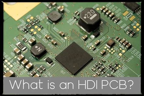
What is an HDI PCB?
HDI PCBs are printed circuit boards that feature higher wiring density than traditional PCBs. They are characterized by their use of microvias, which are small holes drilled through the PCB layers to create interconnections between them. HDI PCBs typically have trace widths and spaces less than 100 μm and hole diameters less than 150 μm.
The following table compares the characteristics of traditional PCBs and HDI PCBs:
| Characteristic | Traditional PCB | HDI PCB |
|---|---|---|
| Trace width/space | ≥ 100 μm | < 100 μm |
| Hole diameter | ≥ 150 μm | < 150 μm |
| Layer count | ≤ 8 layers | ≥ 8 layers |
| Density | Low to medium | High |
HDI PCBs can be classified into different types based on their via structure and the number of HDI layers:
- Type I: Single-sided HDI PCB with microvias from surface to inner layer
- Type II: Double-sided HDI PCB with microvias from surface to inner layer
- Type III: Multi-layer HDI PCB with buried and/or Stacked Microvias
Advantages of HDI PCBs
HDI PCBs offer several advantages over traditional PCBs:
- Miniaturization: HDI PCBs allow for higher component density, enabling the design of smaller and more compact electronic devices.
- Improved signal integrity: The shorter traces and reduced layer count in HDI PCBs result in lower signal attenuation and distortion, leading to better signal integrity.
- Enhanced thermal management: The use of microvias in HDI PCBs improves thermal conductivity, allowing for better heat dissipation and preventing hotspots.
- Reduced EMI: The shorter traces and smaller loop areas in HDI PCBs minimize electromagnetic interference, making them suitable for high-speed and high-frequency applications.
- Cost-effective: Although HDI PCBs may have a higher initial cost, they can be more cost-effective in the long run due to their reduced size and improved performance.

Designing HDI PCBs
Designing HDI PCBs requires careful consideration of several factors to ensure optimal performance and manufacturability. Here are some key aspects to consider when designing HDI PCBs:
Layer Stack-up
The layer stack-up is a critical aspect of HDI PCB design. It determines the number and arrangement of layers, as well as the placement of microvias. A typical HDI PCB Stack-up may include:
- Surface layers: Top and bottom layers where components are placed
- Inner layers: Signal and power/ground layers
- Microvias: Connecting surface layers to inner layers
When designing the layer stack-up, consider the following:
- Signal integrity: Ensure proper impedance control and minimize crosstalk by selecting appropriate dielectric materials and thicknesses.
- Power distribution: Provide adequate power and ground planes to ensure stable power delivery to components.
- Manufacturability: Consider the limitations of the PCB fabrication process, such as minimum via size and drill aspect ratio.
Via Structure
Microvias are a key feature of HDI PCBs, and their structure plays a crucial role in the overall performance and reliability of the board. There are several types of microvias:
- Blind vias: Connecting surface layers to inner layers, but not passing through the entire board thickness.
- Buried vias: Connecting inner layers without reaching the surface layers.
- Stacked vias: Multiple microvias stacked on top of each other to connect multiple layers.
When designing the via structure, consider the following:
- Via size: Smaller vias allow for higher density, but may have limitations in terms of manufacturability and reliability.
- Via-in-pad: Placing vias directly under component pads can save space, but requires careful design to ensure proper solderability and avoid Solder wicking.
- Via fill: Filling vias with conductive or non-conductive materials can improve thermal conductivity and prevent solder wicking, but may increase manufacturing complexity.
Routing and Trace Width
Routing and trace width are critical factors in HDI PCB design, as they directly impact signal integrity and EMI performance. When routing traces, consider the following:
- Trace width and spacing: Narrower traces allow for higher density, but may have higher impedance and be more susceptible to manufacturing defects. Ensure proper spacing between traces to minimize crosstalk.
- Length matching: Match the lengths of critical signal traces to ensure proper timing and avoid signal skew.
- Controlled impedance: Use controlled impedance routing techniques, such as differential pairs and coplanar waveguides, to maintain signal integrity in high-speed designs.
Component Placement
Component placement is another crucial aspect of HDI PCB design, as it affects signal integrity, thermal management, and manufacturability. When placing components, consider the following:
- Placement density: Higher component density allows for smaller board sizes, but may require more complex routing and increase the risk of thermal issues.
- Thermal management: Place high-power components away from sensitive components and provide adequate thermal relief, such as thermal vias or heatsinks.
- Manufacturability: Consider the limitations of the assembly process, such as minimum component spacing and placement tolerances.

Manufacturing HDI PCBs
Manufacturing HDI PCBs requires specialized equipment and processes to achieve the high precision and reliability required. The manufacturing process typically involves the following steps:
- Drilling: Microvias are drilled using laser or mechanical drilling processes, depending on the via size and depth.
- Plating: The microvias are plated with copper to create electrical connections between layers.
- Lamination: The PCB layers are laminated together under high pressure and temperature to form a solid board.
- Patterning: The copper layers are patterned using photolithography and etching processes to create the desired circuit traces.
- Solder mask and silkscreen: A solder mask is applied to protect the copper traces, and a silkscreen is added for component identification and assembly guidance.
To ensure the quality and reliability of HDI PCBs, manufacturers must adhere to strict process controls and quality assurance procedures, such as:
- Cleanliness control: Maintain a clean manufacturing environment to prevent contamination and defects.
- Impedance control: Monitor and control the impedance of the PCB traces to ensure signal integrity.
- Automated optical inspection (AOI): Use AOI systems to detect manufacturing defects, such as shorts, opens, and misalignments.
- Electrical testing: Perform electrical tests, such as continuity and insulation resistance tests, to verify the functionality of the PCB.

Frequently Asked Questions (FAQ)
-
Q: What is the minimum via size achievable in HDI PCBs?
A: The minimum via size in HDI PCBs depends on the manufacturing capabilities of the PCB fabricator. Typically, microvias can have diameters as small as 50-75 μm, but this may vary depending on the specific process and equipment used. -
Q: Can HDI PCBs be used for high-power applications?
A: Yes, HDI PCBs can be used for high-power applications, but special considerations must be made for thermal management. The use of thermal vias, heatsinks, and proper component placement can help dissipate heat and prevent thermal issues. -
Q: Are HDI PCBs more expensive than traditional PCBs?
A: HDI PCBs may have a higher initial cost compared to traditional PCBs due to the specialized manufacturing processes and equipment required. However, they can be more cost-effective in the long run due to their reduced size and improved performance, which can lead to lower system-level costs. -
Q: What are the challenges in designing HDI PCBs?
A: Designing HDI PCBs can be challenging due to the high density and complex routing requirements. Some of the challenges include maintaining signal integrity, managing thermal issues, ensuring manufacturability, and meeting tight tolerances. Designers must have a deep understanding of HDI design principles and work closely with PCB Fabricators to ensure a successful design. -
Q: Can HDI PCBs be reworked or repaired?
A: Reworking or repairing HDI PCBs can be more challenging compared to traditional PCBs due to the smaller features and higher density. Special tools and techniques, such as precision soldering and microscopic inspection, may be required. In some cases, it may be more cost-effective to replace the entire PCB rather than attempting a repair.
Conclusion
HDI PCBs offer numerous advantages over traditional PCBs, including higher density, improved signal integrity, better thermal management, and reduced EMI. However, designing and manufacturing HDI PCBs requires careful consideration of various factors, such as layer stack-up, via structure, routing, and component placement.
To achieve a perfect HDI PCB, designers must have a deep understanding of HDI design principles and work closely with PCB fabricators to ensure manufacturability and reliability. By following best practices and leveraging advanced manufacturing processes, designers can unlock the full potential of HDI technology and create cutting-edge electronic devices that meet the demands of today’s market.


Leave a Reply