Introduction to PCB Printing
Printed Circuit Boards (PCBs) are the backbone of modern electronics. They provide a platform for components to be mounted and connected, forming a complete electronic circuit. PCB printing is the process of creating these boards, which involves several steps and requires careful attention to detail. In this article, we will discuss six important things you should pay special attention to when it comes to custom PCB printing.
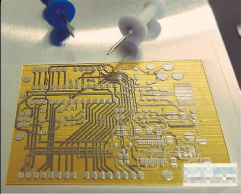
What is PCB Printing?
PCB printing is the process of creating a printed circuit board by depositing conductive ink or etching away unwanted copper to form the desired circuit pattern. This process involves several steps, including:
- Designing the circuit layout
- Printing the circuit pattern onto the board
- Etching away unwanted copper
- Drilling holes for components
- Applying solder mask and silkscreen
- Testing and inspecting the finished board
Why is Custom PCB Printing Important?
Custom PCB printing is important because it allows electronics manufacturers to create boards that are tailored to their specific needs. This can include unique shapes, sizes, and circuit designs that are not available with off-the-shelf boards. Custom PCBs can also be optimized for performance, reliability, and cost-effectiveness.
1. PCB Design and Layout
The first thing to pay special attention to when it comes to custom PCB printing is the design and layout of the board. This involves creating a schematic diagram of the circuit and then translating that into a physical layout that can be printed onto the board.
Schematic Design
The schematic design is the first step in creating a custom PCB. This involves creating a diagram of the electronic circuit, showing all the components and how they are connected. The schematic should be created using a CAD (Computer-Aided Design) program, such as Eagle or KiCad.
PCB Layout
Once the schematic is complete, the next step is to create the physical layout of the board. This involves placing the components on the board and routing the traces (the conductive paths that connect the components). The layout should be optimized for manufacturability, reliability, and performance.
Some important factors to consider when creating the PCB layout include:
- Component placement: Components should be placed in a way that minimizes the length of traces and reduces electromagnetic interference (EMI).
- Trace width and spacing: Traces should be wide enough to handle the expected current flow, and spaced far enough apart to prevent crosstalk and other issues.
- Via placement: Vias (holes that connect different layers of the board) should be placed in a way that minimizes the number of layers needed and improves signal integrity.
Design for Manufacturability (DFM)
When creating the PCB layout, it’s important to keep manufacturability in mind. This means designing the board in a way that makes it easy and cost-effective to manufacture. Some important DFM considerations include:
- Minimum trace width and spacing
- Minimum hole size
- Clearance around the edges of the board
- Solder mask and silkscreen requirements
By designing with manufacturability in mind, you can avoid costly redesigns and delays later in the process.

2. Material Selection
The second thing to pay special attention to when it comes to custom PCB printing is material selection. The materials used to create the board can have a significant impact on its performance, reliability, and cost.
PCB Substrate Materials
The substrate is the base material of the PCB, and it provides the foundation for the conductive layers and components. Common substrate materials include:
- FR-4: A glass-reinforced epoxy laminate that is the most commonly used substrate material for PCBs. It offers good mechanical and electrical properties at a reasonable cost.
- Polyimide: A high-performance substrate material that offers excellent thermal and chemical resistance, making it suitable for harsh environments.
- Aluminum: A metal-core substrate that offers excellent thermal conductivity, making it suitable for high-power applications.
The choice of substrate material will depend on the specific requirements of the application, such as temperature range, mechanical stress, and electrical performance.
Copper Weight
The copper weight refers to the thickness of the copper layer on the PCB. It is typically measured in ounces per square foot (oz/ft²), with common values ranging from 0.5 oz/ft² to 2 oz/ft². Higher copper weights offer better current carrying capacity and improved thermal performance, but also increase the cost and weight of the board.
Solder Mask and Silkscreen
Solder mask and silkscreen are additional layers that are applied to the PCB after the copper traces have been etched. Solder mask is a thin layer of polymer that covers the copper traces, leaving only the pads exposed for soldering. It helps to prevent short circuits and improves the reliability of the board. Silkscreen is a layer of ink that is used to print text and symbols onto the board, such as component labels and logos.
The choice of solder mask and silkscreen colors can affect the visibility and aesthetics of the board. Green is the most common color for solder mask, while white is the most common color for silkscreen.

3. Component Selection and Placement
The third thing to pay special attention to when it comes to custom PCB printing is component selection and placement. The choice and placement of components can have a significant impact on the performance, reliability, and cost of the board.
Component Selection
When selecting components for a custom PCB, it’s important to consider factors such as:
- Functionality: The component must be able to perform the required function within the circuit.
- Compatibility: The component must be compatible with the other components in the circuit and with the PCB itself.
- Availability: The component must be readily available from suppliers, with a reliable supply chain.
- Cost: The component must be cost-effective, considering both the unit cost and the total cost of ownership.
It’s also important to consider the environmental requirements of the application, such as temperature range, humidity, and vibration, and to select components that are rated for those conditions.
Component Placement
Once the components have been selected, the next step is to place them on the PCB layout. The placement of components can affect the performance and reliability of the board, as well as the ease of assembly and maintenance.
Some important factors to consider when placing components include:
- Electrical performance: Components should be placed in a way that minimizes the length of traces and reduces electromagnetic interference (EMI).
- Thermal performance: Components that generate a lot of heat should be placed in a way that allows for adequate cooling, such as near the edge of the board or with sufficient spacing between them.
- Mechanical stress: Components that are subject to mechanical stress, such as connectors or switches, should be placed in a way that minimizes the stress on the board and the components themselves.
- Assembly and maintenance: Components should be placed in a way that allows for easy assembly and maintenance, with sufficient space for soldering and inspection.
By carefully selecting and placing components, you can optimize the performance, reliability, and cost of the custom PCB.

4. Manufacturing Process
The fourth thing to pay special attention to when it comes to custom PCB printing is the manufacturing process itself. The quality and consistency of the manufacturing process can have a significant impact on the final product.
PCB Fabrication
PCB fabrication involves several steps, including:
- Printing the circuit pattern onto the substrate using a photoresist and exposing it to light
- Etching away the unwanted copper using a chemical solution
- Drilling holes for vias and component leads
- Applying solder mask and silkscreen
- Cutting the board to its final shape
Each of these steps must be carefully controlled to ensure a high-quality final product. Factors such as the type of photoresist, the etching solution, and the drilling parameters can all affect the accuracy and reliability of the board.
Assembly
Once the PCB has been fabricated, the next step is to assemble the components onto the board. This typically involves soldering the components onto the pads using a reflow oven or a wave soldering machine.
The quality of the assembly process can be affected by factors such as the type of solder used, the temperature and duration of the reflow process, and the cleanliness of the board and components.
Testing and Inspection
After assembly, the board must be tested and inspected to ensure that it meets the required specifications. This typically involves a combination of automated optical inspection (AOI), X-ray inspection, and electrical testing.
AOI uses cameras and image processing software to inspect the board for defects such as missing components, solder bridges, and incorrect component placement. X-ray inspection can be used to detect hidden defects such as voids in the solder joints or broken traces. Electrical testing involves applying power to the board and measuring its performance against a set of predefined criteria.
By carefully controlling each step of the manufacturing process and performing thorough testing and inspection, you can ensure a high-quality final product that meets your requirements.
5. Cost Considerations
The fifth thing to pay special attention to when it comes to custom PCB printing is cost. The cost of a custom PCB can vary widely depending on factors such as the size and complexity of the board, the materials used, and the manufacturing process.
Board Size and Complexity
The size and complexity of the board are two of the biggest factors that affect the cost of a custom PCB. Larger boards with more layers and more complex designs will generally be more expensive than smaller, simpler boards.
Some ways to reduce the cost of a custom PCB include:
- Minimizing the number of layers: Each additional layer adds cost and complexity to the board. By minimizing the number of layers, you can reduce the cost of the board without sacrificing performance.
- Using standard sizes: Many PCB Manufacturers offer standard board sizes that are optimized for their manufacturing process. By using a standard size, you can reduce the cost and lead time of the board.
- Simplifying the design: By simplifying the design of the board, you can reduce the number of components and traces needed, which can reduce the cost and complexity of the board.
Material Costs
The cost of the materials used to create the PCB can also have a significant impact on the overall cost of the board. Some ways to reduce material costs include:
- Using standard materials: Many PCB manufacturers offer standard materials that are optimized for their manufacturing process. By using standard materials, you can reduce the cost and lead time of the board.
- Minimizing the use of expensive materials: Some materials, such as high-performance substrates or thick copper layers, can significantly increase the cost of the board. By minimizing the use of these materials, you can reduce the overall cost of the board.
- Optimizing the design for manufacturability: By designing the board with manufacturability in mind, you can reduce the amount of material waste and improve the yield of the manufacturing process, which can reduce the overall cost of the board.
Quantity and Lead Time
The quantity and lead time of the order can also affect the cost of a custom PCB. In general, larger quantities and longer lead times will result in lower per-unit costs, while smaller quantities and shorter lead times will result in higher per-unit costs.
Some ways to optimize the quantity and lead time of a custom PCB order include:
- Planning ahead: By planning your PCB needs well in advance, you can take advantage of longer lead times and larger order quantities to reduce the per-unit cost of the boards.
- Working with a reliable supplier: By working with a reliable PCB supplier that can consistently meet your quality and delivery requirements, you can reduce the risk of delays and quality issues that can increase the overall cost of the project.
- Considering the total cost of ownership: When evaluating the cost of a custom PCB, it’s important to consider the total cost of ownership, including not just the initial purchase price but also the cost of assembly, testing, and any potential rework or scrap.
6. Communication and Collaboration
The sixth and final thing to pay special attention to when it comes to custom PCB printing is communication and collaboration. Effective communication and collaboration between the design team, the manufacturing team, and the end user can help to ensure a successful project outcome.
Design Reviews
Design reviews are an important part of the PCB design process, and they provide an opportunity for all stakeholders to review and provide feedback on the design before it is sent for manufacturing.
Some best practices for design reviews include:
- Involving all stakeholders: Design reviews should involve representatives from the design team, the manufacturing team, and the end user to ensure that all perspectives and requirements are considered.
- Using a structured review process: A structured review process, such as a design review checklist or a formal design review meeting, can help to ensure that all important aspects of the design are reviewed and discussed.
- Documenting the results: The results of the design review should be documented and shared with all stakeholders to ensure that everyone is on the same page and that any required changes are implemented.
Manufacturing Feedback
Feedback from the manufacturing team can be invaluable in optimizing the design for manufacturability and reducing the risk of delays or quality issues.
Some best practices for manufacturing feedback include:
- Early involvement: The manufacturing team should be involved in the design process as early as possible to provide feedback on the manufacturability of the design.
- Regular communication: Regular communication between the design team and the manufacturing team can help to identify and resolve any issues quickly and efficiently.
- Continuous improvement: The manufacturing team should be encouraged to provide ongoing feedback and suggestions for improvement, even after the initial design is complete.
End User Feedback
Feedback from the end user can help to ensure that the custom PCB meets their specific needs and requirements.
Some best practices for end user feedback include:
- Early involvement: The end user should be involved in the design process as early as possible to provide input on their specific requirements and use case.
- Prototype testing: Providing the end user with a prototype of the custom PCB can help to identify any issues or areas for improvement before the final product is manufactured.
- Ongoing support: Providing ongoing support and communication with the end user can help to ensure that the custom PCB continues to meet their needs over time.
By fostering effective communication and collaboration between all stakeholders, you can help to ensure a successful custom PCB project that meets the needs of all parties involved.
Frequently Asked Questions (FAQ)
- What is the typical turnaround time for a custom PCB order?
-
The turnaround time for a custom PCB order can vary depending on the complexity of the design, the materials used, and the manufacturing process. Typical turnaround times range from 2-3 days for simple designs to 2-3 weeks for more complex designs.
-
What is the minimum order quantity for a custom PCB?
-
The minimum order quantity for a custom PCB can vary depending on the manufacturer and the specific design requirements. Some manufacturers may offer low minimum order quantities of just a few boards, while others may require larger minimum orders of 100 or more boards.
-
What file formats are typically required for a custom PCB design?
-
The most common file formats for a custom PCB design include Gerber files (.gbr), drill files (.drl), and pick-and-place files (.csv or .txt). Some manufacturers may also require additional files such as bill of materials (BOM) or assembly drawings.
-
Can I specify custom silkscreen or solder mask colors for my PCB?
-
Yes, most PCB manufacturers offer a range of standard and custom silkscreen and solder mask colors to choose from. Custom colors may require additional setup fees or minimum order quantities.
-
What is the typical cost per unit for a custom PCB?
- The cost per unit for a custom PCB can vary widely depending on factors such as the size and complexity of the board, the materials used, and the order quantity. Typical costs can range from a few dollars per board for simple designs and large quantities to several hundred dollars per board for complex designs and small quantities. It’s important to work with your PCB supplier to understand the specific cost drivers for your project and to optimize the design and order quantity for cost-effectiveness.
Conclusion
In conclusion, custom PCB printing is a complex process that requires careful attention to detail in order to ensure a high-quality final product. By paying special attention to the six key areas discussed in this article – PCB design and layout, material selection, component selection and placement, manufacturing process, cost considerations, and communication and collaboration – you can help to optimize the performance, reliability, and cost-effectiveness of your custom PCB project.
Some key takeaways to keep in mind include:
- Designing for manufacturability and reliability, not just functionality
- Carefully selecting materials and components based on the specific requirements of the application
- Controlling each step of the manufacturing process to ensure consistency and quality
- Considering the total cost of ownership, not just the initial purchase price
- Fostering effective communication and collaboration between all stakeholders throughout the project lifecycle
By following these best practices and working with a reliable PCB supplier, you can help to ensure the success of your custom PCB project and bring your electronic product vision to life.


Leave a Reply