Understanding the Basics of PCB Fabrication Drawings
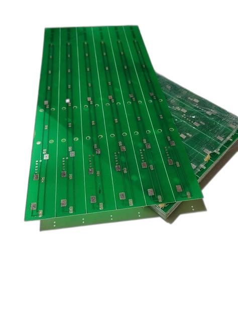
A PCB fabrication drawing, also known as a PCB manufacturing drawing or fab drawing, is a detailed blueprint that contains all the information needed to manufacture a printed circuit board. It specifies the PCB’s physical dimensions, materials, layer stackup, drill holes, tolerances, markings, and other critical parameters.
Being able to read and interpret a PCB fabrication drawing is an essential skill for hardware engineers, PCB designers, and electronics manufacturers. It allows you to communicate your design intent clearly to the fab house and ensure the PCB is built to your exact specifications.
In this article, we’ll cover everything you need to know about PCB fabrication drawings, including:
- The key elements of a PCB fab drawing
- How to read the physical dimensions and tolerances
- Understanding the layer stackup and materials
- Interpreting drill hole and Via information
- Decoding the surface finish and silkscreen markings
- Frequently asked questions about PCB fab drawings
By the end, you’ll be able to confidently read any PCB fabrication drawing and work effectively with your manufacturing partners to bring your electronics designs to life. Let’s dive in!
The Anatomy of a PCB Fabrication Drawing
A typical PCB fabrication drawing includes several views and sections that detail the board’s physical construction. Here are the main components you’ll find:
Mechanical Drawing View
The mechanical drawing view is a top-down view of the PCB that shows its physical outline, dimensions, and major features. It specifies the board size, shape, and any cutouts, notches, or unusual contours.
The dimensions are usually given in both metric (mm) and imperial (inch) units. They indicate the board’s length, width, and thickness, as well as the size and position of any holes, slots, or other mechanical features.
Tolerances are also specified for each dimension, typically in the format of “nominal ± tolerance.” For example, a dimension might read “100mm ± 0.2mm,” meaning the actual size can vary by up to 0.2mm larger or smaller than the nominal 100mm. Tighter tolerances generally cost more to manufacture.
Layer Stackup Section
The layer stackup section shows a cross-section view of the PCB’s internal structure. It specifies the number of copper layers, their arrangement, and the insulating materials between them.
Each copper layer is labeled with a name (e.g. Top, Bottom, Inner1, Inner2) and a function (e.g. signal, power, ground). The insulating layers are also labeled with their material type (e.g. FR-4, Rogers, polyimide) and thickness.
The stackup also specifies the total thickness of the PCB, which is the sum of all the layer thicknesses. It’s important to note that the actual thickness may vary slightly due to manufacturing tolerances.
Here’s an example 4-layer PCB stackup:
| Layer | Material | Thickness (mm) | Tolerance (±mm) |
|---|---|---|---|
| Top | Copper | 0.035 | 0.005 |
| Core | FR-4 | 0.2 | 0.05 |
| Inner1 | Copper | 0.0175 | 0.005 |
| Core | FR-4 | 0.4 | 0.05 |
| Inner2 | Copper | 0.0175 | 0.005 |
| Core | FR-4 | 0.2 | 0.05 |
| Bottom | Copper | 0.035 | 0.005 |
| Total | 1.6 | 0.1 |
Drill Chart and Drill Drawing
The drill chart and drill drawing specify all the holes that need to be drilled in the PCB, including:
- Plated through-holes for component leads
- Unplated mounting holes for screws or standoffs
- Via holes for connecting different layers
- Slot holes for connectors or switches
The drill chart lists each hole type with a unique symbol, diameter, tolerance, and plating requirements (if any). The drill drawing shows the location of each hole on the board using the corresponding symbols.
Designers need to be careful to specify the correct hole sizes for component pins, or else there may be assembly issues. Vias also need to be sized appropriately for their current-carrying requirements and to avoid manufacturing defects.
Legend and Marking Callouts
PCB fabrication drawings also specify the legend and markings that need to be printed or silk-screened onto the board. These include:
- Component outlines and reference designators
- Pin 1 indicators and polarity marks
- Test points and fiducial marks
- Company logos, part numbers, and certifications
- Warning labels and user instructions
The drawing will show the size, position, and content of each marking, usually on a separate layer. It’s important to check that the markings are legible and won’t be obscured by components or solder mask.
Some designs may also require serialized markings or barcodes for traceability. In that case, the drawing should specify the serialization format and provide a blank area for the fab house to add the variable data.

Interpreting Material Specifications
In addition to the stackup materials, a PCB fabrication drawing also specifies the materials for the soldermask, silkscreen, and surface finish. These are usually called out in a separate table or list.
Soldermask
The soldermask is the protective coating that covers the copper traces on the outer layers of the PCB. It prevents accidental short circuits and provides electrical insulation.
The drawing will specify the soldermask color (green, red, blue, black, white, or custom) and the material type. The most common soldermask material is liquid photoimageable (LPI) epoxy, which is applied via silkscreen printing and then photolithographically patterned and cured.
Silkscreen
The silkscreen is the white or colored ink that’s used to print text and graphics on the PCB surface. It’s typically applied on top of the soldermask.
The drawing will specify the silkscreen color and the ink type. The standard colors are white and black, but other colors like yellow or gray are sometimes used for better contrast or readability.
Surface Finish
The surface finish is the coating applied to the exposed copper pads and contacts on the PCB. It serves several purposes:
– Protecting the copper from oxidation and corrosion
– Enhancing the solderability of the pads
– Improving the durability and shelf life of the PCB
– Meeting RoHS or other environmental regulations
There are several common types of PCB surface finishes, each with their own advantages and trade-offs. The fabrication drawing will specify which finish to use based on the design requirements and cost targets.
The most popular surface finish options include:
| Finish | Composition | Pros | Cons |
|---|---|---|---|
| HASL (SnPb) | Tin-lead alloy | Low cost, good solderability, easy rework | Not RoHS compliant, uneven surface |
| Lead-free HASL (pure Sn) | Pure tin | Low cost, good solderability, RoHS compliant | Uneven surface, tin whiskers |
| ENIG | Electroless nickel / immersion gold | Flat surface, good solderability, aluminum wire bonding | Higher cost, black pad, weak solder joints |
| ENEPIG | Electroless nickel / electroless palladium / immersion gold | Flat surface, good solderability, gold wire bonding | Highest cost, process complexity |
| OSP | Organic solderability preservative | Low cost, flat surface, quick turn | Poor shelf life, incompatible with some assembly processes |
| Immersion silver | Pure silver | Low cost, flat surface, good solderability | Tarnishing, incompatible with some components |
| Immersion tin | Pure tin | Low cost, flat surface, good solderability | Tin whiskers, shelf life |
The fabrication drawing should call out the specific surface finish, along with any special requirements like ENIG thickness, OSP type, or Immersion silver aging.

Reading Fabrication Notes and Callouts
Most fabrication drawings will also include notes and callouts that provide additional manufacturing instructions or design constraints. These are usually located around the edges of the drawing or on a separate sheet.
Some common fabrication notes include:
– PCB material grade and Tg requirements
– Copper weight and trace/space design rules
– Drill bit sizes and hit counts
– Impedance control requirements
– Hole plugging or via filling
– Panelization and array design
– Electrical test and inspection criteria
– Packaging and shipping instructions
It’s important to read through all the fab notes carefully and make sure they match your design intent. Any discrepancies or ambiguities should be resolved with the fab house before starting production.

Frequently Asked Questions
What file format should I use for my PCB fabrication drawing?
The most common file format for PCB fabrication drawings is Gerber RS-274X. This is a vector image format that specifies each copper layer, drill layer, and silkscreen layer separately.
Gerber files are usually accompanied by an NC drill file (Excellon format) that contains the drill hole locations and sizes. Some designs may also include a pick-and-place file that specifies the component locations for automated assembly.
Other popular fabrication file formats include ODB++ (Mentor Graphics) and IPC-2581 (Nimbic). These are intelligent CAD formats that include net connectivity information in addition to the layer images.
How do I choose the right layer stackup for my design?
The layer stackup depends on the complexity of your circuit, the signal integrity requirements, and the cost targets. Here are some general guidelines:
- Simple, low-density boards can use 1 or 2 layers
- Most moderate-complexity boards use 4 layers (signal, ground, power, signal)
- High-speed digital boards may use 6 or 8 layers with dedicated signal and plane layers
- Complex, high-density boards can go up to 16 or more layers
It’s best to work with your fab house to determine the optimal stackup for your design. They can help you choose the right materials, thicknesses, and spacings to meet your electrical and mechanical requirements.
What are the most common PCB materials?
The most common PCB material is FR-4, a woven fiberglass fabric impregnated with an epoxy resin. It’s low-cost, durable, and has good mechanical and electrical properties for most applications.
For high-speed digital designs, lower-loss materials like Rogers or Isola may be used to improve signal integrity. For high-temperature or harsh-environment applications, polyimide or ceramics may be used for their thermal and chemical stability.
There are also specialized materials for flexible and rigid-flex PCBs, metal-core PCBs, and RF/microwave PCBs. The fabrication drawing should specify the exact material grade and properties required.
How tight should I make my PCB tolerances?
In general, tighter tolerances will result in higher manufacturing costs and longer lead times. It’s best to use the loosest tolerances that still meet your functional and reliability requirements.
For most PCBs, a dimensional tolerance of ±0.2mm is sufficient. Tighter tolerances of ±0.1mm or ±0.05mm may be needed for high-density designs or precise mechanical fits.
Copper feature tolerances (trace width, spacing, annular ring) are typically specified as a percentage of the nominal value, such as ±10% or ±20%. Tighter tolerances may be needed for high-current traces or fine-pitch components.
Drill hole tolerances are usually specified as a ±mm value, such as ±0.1mm or ±0.05mm. Tighter hole tolerances may be needed for press-fit pins or plated through-holes with high aspect ratios.
How do I specify the solder mask and silkscreen colors?
The fabrication drawing should specify the solder mask and silkscreen colors using either:
- Pantone color codes (e.g. Pantone 354C for green solder mask)
- RAL color codes (e.g. RAL 9005 for black silkscreen)
- Custom color swatches or samples
It’s important to choose colors that provide good contrast and readability for your design. The fab house can provide guidance on the available color options and their suitability for your application.
Conclusion
Reading a PCB fabrication drawing may seem daunting at first, but with practice it becomes second nature. By understanding the key elements of the drawing and how they relate to the manufacturing process, you can ensure that your PCBs are built to your exact specifications every time.
Remember to always work closely with your fab house and communicate your requirements clearly through the fabrication drawing. And don’t be afraid to ask questions if anything is unclear – a little extra effort upfront can save a lot of headaches and delays down the line.
With these tips in mind, you’re ready to start creating PCB designs that are optimized for manufacturability, reliability, and performance. Happy designing!


Leave a Reply