What is Solder Mask?
Solder mask, also known as solder resist or solder stop, is a thin layer of polymer applied to the copper traces of a printed circuit board (PCB). Its primary purpose is to protect the copper traces from oxidation, prevent solder bridges from forming between closely spaced pads, and provide electrical insulation. Solder mask also helps to improve the overall appearance of the PCB by providing a uniform color, typically green, red, blue, black, or yellow.
Composition of Solder Mask
Solder mask is typically composed of a photoimageable polymer, such as epoxy or acrylic, that is sensitive to ultraviolet (UV) light. The polymer is mixed with various additives, including:
- Pigments for color
- Fillers for improved mechanical properties
- Photoinitiators for UV sensitivity
- Stabilizers for long-term durability
Application Process
The application of solder mask involves several steps:
-
Cleaning: The PCB surface is thoroughly cleaned to remove any contaminants that may interfere with the adhesion of the solder mask.
-
Application: The liquid solder mask is applied to the PCB surface using various methods, such as screen printing, spray coating, or curtain coating.
-
Drying: The coated PCB is then dried to remove any excess solvent from the solder mask.
-
Exposure: The dried solder mask is exposed to UV light through a photomask, which selectively hardens the exposed areas.
-
Developing: The unexposed areas of the solder mask are then removed using a chemical developer, leaving behind the desired pattern.
-
Curing: Finally, the PCB is subjected to a high-temperature curing process to fully crosslink the solder mask and enhance its mechanical and chemical properties.
Types of Solder Mask
There are two main types of solder mask: liquid photoimageable (LPI) and dry film photoimageable (DFPI).
Liquid Photoimageable (LPI) Solder Mask
LPI solder mask is applied to the PCB surface in liquid form and then exposed to UV light to create the desired pattern. LPI solder mask offers several advantages:
- Excellent conformity to surface features
- Thin and uniform coating thickness
- High resolution and fine feature definition
- Wide range of available colors
However, LPI solder mask also has some disadvantages:
- Longer processing time due to multiple steps involved
- Higher equipment and material costs
- Potential for air bubbles or pinholes in the coating
Dry Film Photoimageable (DFPI) Solder Mask
DFPI solder mask is supplied as a solid film that is laminated onto the PCB surface and then exposed to UV light. DFPI solder mask offers several advantages:
- Faster processing time due to fewer steps involved
- Lower equipment and material costs
- Consistent thickness and uniformity
- Minimal risk of air bubbles or pinholes
However, DFPI solder mask also has some disadvantages:
- Limited conformity to surface features
- Thicker coating compared to LPI
- Lower resolution and feature definition
- Limited color options

Properties of Solder Mask
Solder mask must possess several key properties to effectively protect the PCB and ensure reliable performance:
Adhesion
Solder mask must adhere strongly to the PCB surface to prevent delamination or peeling during assembly or use. Good adhesion is critical for maintaining the integrity of the solder mask and protecting the underlying copper traces.
Electrical Insulation
Solder mask must provide adequate electrical insulation between adjacent copper traces to prevent short circuits and ensure proper functioning of the PCB. The insulation properties of solder mask are typically measured by its dielectric strength and surface insulation resistance.
Chemical Resistance
Solder mask must be resistant to various chemicals used in the PCB manufacturing process, such as fluxes, solvents, and cleaning agents. It should also be resistant to environmental factors such as moisture, salt spray, and UV radiation to ensure long-term durability.
Thermal Stability
Solder mask must be able to withstand the high temperatures encountered during the soldering process without degrading or losing its properties. It should also have a low coefficient of thermal expansion (CTE) to minimize stress on the PCB during thermal cycling.
Flame Retardancy
Solder mask should be flame retardant to prevent the spread of fire in case of a short circuit or other electrical fault. Flame retardancy is typically achieved by incorporating halogen-free flame retardants into the solder mask formulation.

Solder Mask Colors
Solder mask is available in a wide range of colors, with green being the most common. However, other colors such as red, blue, black, and yellow are also frequently used. The choice of color is often based on aesthetic preferences, but it can also serve functional purposes:
- Green: The most common color, green solder mask provides good contrast with copper traces and is easy on the eyes.
- Red: Often used for high-voltage or power circuits to provide a visual warning.
- Blue: Sometimes used for prototype or pre-production PCBs to distinguish them from final production boards.
- Black: Provides a sleek, modern appearance and can help to hide surface blemishes or imperfections.
- Yellow: Often used for high-density PCBs or those with fine pitch components to provide better visibility during assembly.
| Color | Advantages | Disadvantages |
|---|---|---|
| Green | Good contrast, easy on the eyes | May not be suitable for certain applications |
| Red | Provides visual warning for high-voltage or power circuits | May be too bright or distracting in some cases |
| Blue | Distinguishes prototype or pre-production PCBs | May not provide sufficient contrast with copper traces |
| Black | Sleek appearance, hides surface blemishes | May make it difficult to inspect solder joints |
| Yellow | Provides better visibility for high-density or fine pitch PCBs | May not be as aesthetically pleasing as other colors |

Solder Mask Design Considerations
When designing a PCB with solder mask, several key factors must be considered to ensure optimal performance and manufacturability:
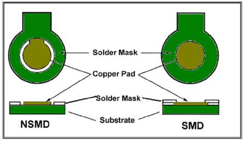
Solder Mask Clearance
Solder mask clearance refers to the distance between the edge of a copper pad and the opening in the solder mask. Adequate clearance is necessary to ensure that the solder mask does not interfere with the soldering process or the formation of a reliable solder joint. The minimum solder mask clearance depends on the size of the pad and the capabilities of the PCB manufacturer, but a typical value is 0.05 mm (2 mil).
Solder Mask Expansion
Solder mask expansion refers to the tendency of the solder mask to expand or contract during the curing process, which can cause misalignment between the solder mask and the underlying copper features. To compensate for this, the solder mask artwork must be adjusted to account for the expected expansion or contraction. The amount of adjustment depends on the specific solder mask material and the curing process used by the PCB manufacturer.
Solder Mask Sliver
Solder mask sliver refers to a thin strip of exposed copper between two adjacent solder mask openings. Slivers can occur when the spacing between pads is too small or when the solder mask artwork is not properly aligned. Slivers can cause short circuits or other reliability issues, so they must be avoided by ensuring adequate spacing between pads and careful alignment of the solder mask artwork.
Solder Mask Dams
Solder mask dams are small strips of solder mask that are placed between adjacent pads to prevent solder bridging. Dams are especially important for fine-pitch components or high-density PCBs where the spacing between pads is very small. The width of the dam depends on the pad spacing and the capabilities of the PCB manufacturer, but a typical value is 0.1 mm (4 mil).
Advantages of Solder Mask
Solder mask offers several key advantages for PCBs:
Protection of Copper Traces
Solder mask protects the copper traces on the PCB from oxidation, corrosion, and mechanical damage. This helps to ensure the long-term reliability and functionality of the PCB.
Prevention of Solder Bridging
Solder mask prevents solder from bridging between closely spaced pads during the soldering process. This is especially important for high-density PCBs or those with fine-pitch components.
Improved Appearance
Solder mask provides a uniform, professional appearance to the PCB, which can be important for consumer products or other applications where aesthetics are a concern.
Enhanced Durability
Solder mask helps to improve the durability of the PCB by protecting it from environmental factors such as moisture, dust, and UV radiation. This can help to extend the lifespan of the PCB and reduce the risk of failures.
Disadvantages of Solder Mask
Despite its many advantages, solder mask also has some potential disadvantages:
Increased Cost
The application of solder mask adds an additional step to the PCB manufacturing process, which can increase the overall cost of the PCB.
Longer Lead Times
The solder mask application process can also increase the lead time for PCB production, especially for complex designs or those requiring multiple layers of solder mask.
Potential for Defects
Solder mask defects such as pinholes, bubbles, or incomplete coverage can occur during the application process, which can compromise the protection and reliability of the PCB.
Limited Repairability
Once solder mask has been applied to a PCB, it can be difficult to repair or rework the board without damaging the solder mask or the underlying copper features.
Frequently Asked Questions (FAQ)
1. What is the difference between solder mask and conformal coating?
Solder mask and conformal coating are both protective coatings applied to PCBs, but they serve different purposes. Solder mask is applied before the soldering process and is designed to protect the copper traces and prevent solder bridging. Conformal coating, on the other hand, is applied after the soldering process and is designed to protect the entire PCB from environmental factors such as moisture, dust, and chemicals.
2. Can solder mask be removed from a PCB?
Yes, solder mask can be removed from a PCB using various methods such as chemical stripping, laser ablation, or mechanical abrasion. However, removing solder mask can be a delicate and time-consuming process that requires specialized equipment and expertise.
3. How does solder mask affect the electrical properties of a PCB?
Solder mask can affect the electrical properties of a PCB in several ways. It can increase the dielectric constant and dissipation factor of the PCB, which can affect the signal integrity and high-frequency performance. Solder mask can also increase the surface insulation resistance and dielectric strength of the PCB, which can improve its electrical safety and reliability.
4. What is the typical thickness of solder mask?
The typical thickness of solder mask ranges from 0.01 mm to 0.03 mm (0.4 mil to 1.2 mil), depending on the specific material and application method used. LPI solder mask tends to be thinner than DFPI solder mask, with a typical thickness of 0.01 mm to 0.02 mm (0.4 mil to 0.8 mil).
5. Can solder mask be used on Flexible PCBs?
Yes, solder mask can be used on flexible PCBs, but it requires specialized materials and application methods to ensure adequate flexibility and adhesion. Flexible solder mask is typically made from polyimide or other flexible polymers and is applied using a screen printing or spray coating process. The thickness and cure temperature of the solder mask must also be carefully controlled to prevent cracking or delamination during flexing.
Conclusion
Solder mask is a critical component of modern PCBs that provides essential protection, insulation, and aesthetic benefits. By understanding the composition, application process, properties, and design considerations of solder mask, PCB designers and manufacturers can ensure the reliability, functionality, and durability of their products. While solder mask does have some potential disadvantages, such as increased cost and lead time, its many advantages make it an indispensable part of the PCB manufacturing process.


Leave a Reply