Introduction to Solder Mask Dam
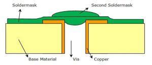
Solder mask dam is an important feature in printed circuit board (PCB) design and manufacturing. It involves creating a barrier or “dam” around specific areas of the PCB using solder mask material. The purpose of solder mask dam is to contain the flow of liquid solder during the assembly process, preventing it from spreading to unwanted areas of the board.
Solder mask, also known as solder resist or solder stop, is a thin layer of polymer material applied to the copper traces of a PCB. Its primary function is to protect the copper from oxidation and prevent accidental short circuits by acting as an insulating layer. Solder mask also provides a surface for applying component labels and other markings.
Key Functions of Solder Mask Dam
- Containment of solder flow
- Protection of sensitive areas on the PCB
- Improving the reliability of solder joints
- Enhancing the overall aesthetics of the PCB
How Solder Mask Dam Works
Solder mask dam works by creating a physical barrier around specific areas of the PCB where solder needs to be contained. This barrier is typically created using the same solder mask material used to cover the rest of the board. The dam is designed to be slightly higher than the surrounding solder mask, effectively creating a wall that prevents molten solder from flowing beyond the desired area.
The Solder Mask Dam Process
-
PCB Design: The location and dimensions of the solder mask dam are determined during the PCB design phase. The dam is typically placed around components that require precise solder control, such as fine-pitch surface mount devices (SMDs) or connectors.
-
Solder Mask Application: The solder mask material is applied to the PCB using various methods, such as screen printing, liquid photoimageable (LPI) solder mask, or dry film solder mask. The dam is created by selectively applying a thicker layer of solder mask in the desired areas.
-
Solder Mask Curing: After application, the solder mask undergoes a curing process to harden and adhere to the PCB surface. This process typically involves exposure to UV light and/or heat, depending on the type of solder mask used.
-
PCB Assembly: During the assembly process, components are placed on the PCB, and the board is subjected to a solder reflow process. The solder mask dam contains the molten solder within the designated areas, ensuring precise solder joint formation.

Advantages of Using Solder Mask Dam
Using solder mask dam in PCB manufacturing offers several advantages:
-
Improved Solder Joint Reliability: By containing the solder flow, solder mask dam helps ensure that the right amount of solder is deposited on each pad. This leads to stronger, more reliable solder joints and reduces the risk of bridging or short circuits.
-
Better Control Over Solder Volume: Solder mask dam allows for precise control over the volume of solder used in each joint. This is particularly important for fine-pitch components and high-density PCB layouts, where excess solder can cause issues.
-
Protection of Sensitive Components: Some components, such as RF shields or connectors, require a precise amount of solder for optimal performance. Solder mask dam helps protect these sensitive areas from excessive solder flow, ensuring the components function as intended.
-
Enhanced PCB Aesthetics: By creating clean, well-defined solder joints, solder mask dam can improve the overall appearance of the PCB. This is particularly important for consumer electronics and other products where visual appeal is a key consideration.

Challenges and Considerations
While solder mask dam offers many benefits, there are also some challenges and considerations to keep in mind:
-
Design Complexity: Incorporating solder mask dam into a PCB design can add complexity and require careful planning. Designers must ensure that the dam dimensions are appropriate for the specific components and solder paste being used.
-
Manufacturing Challenges: Creating a consistent and reliable solder mask dam requires precise control over the solder mask application process. Variations in dam height or thickness can lead to inconsistent solder flow and potentially impact the reliability of the solder joints.
-
Cost Considerations: Implementing solder mask dam may increase the overall cost of PCB manufacturing, as it requires additional processing steps and materials. However, the benefits of improved solder joint reliability and reduced defects often outweigh the incremental cost.
-
Compatibility with Solder Paste: The effectiveness of solder mask dam depends on the compatibility between the solder mask material and the solder paste being used. Some solder pastes may exhibit different flow characteristics or wetting properties, which can impact the performance of the dam.

Best Practices for Implementing Solder Mask Dam
To ensure the successful implementation of solder mask dam in PCB manufacturing, consider the following best practices:
-
Collaborate with PCB Manufacturers: Work closely with your PCB manufacturer to discuss your solder mask dam requirements. They can provide guidance on the best dam dimensions, materials, and manufacturing processes for your specific application.
-
Consider Component Placement: When designing your PCB layout, consider the placement of components in relation to the solder mask dam. Ensure that there is sufficient clearance between the dam and adjacent components to avoid any interference during assembly.
-
Use Appropriate Solder Mask Materials: Select a solder mask material that is compatible with your solder paste and offers good flow control properties. Consult with your PCB manufacturer or solder mask supplier for recommendations based on your specific requirements.
-
Perform Thorough Testing: Before mass production, conduct thorough testing to validate the effectiveness of your solder mask dam design. This may include visual inspections, x-ray analysis, and functional testing to ensure the reliability of the solder joints.
-
Monitor Process Control: Implement strict process control measures during PCB manufacturing to ensure consistent solder mask dam application. This may involve regular inspections, measurements, and statistical process control (SPC) techniques to identify and correct any deviations.
Solder Mask Dam vs. Other Solder Containment Methods
Solder mask dam is not the only method used for containing solder flow on PCBs. Other techniques include:
-
Solder Thieves: Solder thieves are small pads or traces placed adjacent to the main solder pads. They attract excess solder away from the main pads, helping to control the amount of solder deposited on each joint.
-
Solder Dams: Similar to solder mask dam, solder dams are physical barriers created using non-conductive materials, such as epoxy or ceramic. They are typically used in high-temperature or harsh environments where solder mask may not be suitable.
-
Selective Solder Masks: Selective solder masks involve applying solder mask only to specific areas of the PCB, leaving other areas exposed. This technique can be used to create localized solder containment without the need for a full solder mask dam.
The choice of solder containment method depends on various factors, including the specific application, PCB design, manufacturing process, and cost considerations.
Future Trends and Developments
As PCB technology continues to evolve, so too will the techniques used for solder containment and control. Some future trends and developments in this area may include:
-
Advanced Solder Mask Materials: The development of new solder mask materials with improved flow control, thermal stability, and compatibility with advanced packaging techniques.
-
3D Printing of Solder Mask Dams: The use of 3D printing technology to create custom solder mask dams with complex geometries and precise dimensions.
-
Automated Inspection Systems: The implementation of automated inspection systems that can detect and analyze solder mask dam defects in real-time, enabling faster and more reliable quality control.
-
Integration with Advanced Packaging Technologies: The adaptation of solder mask dam techniques to accommodate advanced packaging technologies, such as wafer-level packaging (WLP) and 3D integrated circuits (3D-ICs).
Frequently Asked Questions (FAQ)
-
What is the purpose of solder mask dam?
A: The purpose of solder mask dam is to contain the flow of liquid solder during the PCB assembly process, preventing it from spreading to unwanted areas of the board. -
How is solder mask dam created on a PCB?
A: Solder mask dam is typically created by selectively applying a thicker layer of solder mask material around the desired areas during the solder mask application process. -
What are the benefits of using solder mask dam?
A: The benefits of using solder mask dam include improved solder joint reliability, better control over solder volume, protection of sensitive components, and enhanced PCB aesthetics. -
Can solder mask dam be used with all types of solder paste?
A: The effectiveness of solder mask dam depends on the compatibility between the solder mask material and the solder paste being used. Some solder pastes may exhibit different flow characteristics or wetting properties, which can impact the performance of the dam. -
Are there any alternatives to solder mask dam for solder containment?
A: Yes, other solder containment methods include solder thieves, solder dams, and selective solder masks. The choice of method depends on factors such as the specific application, PCB design, manufacturing process, and cost considerations.
Conclusion
Solder mask dam is a critical feature in PCB design and manufacturing, offering numerous benefits for solder control and reliability. By creating a physical barrier around specific areas of the PCB, solder mask dam helps ensure precise solder joint formation, protects sensitive components, and enhances the overall aesthetics of the board.
Implementing solder mask dam requires careful consideration of design requirements, manufacturing processes, and material compatibility. By collaborating with PCB manufacturers, using appropriate materials, and following best practices, designers and engineers can successfully incorporate solder mask dam into their PCB designs.
As PCB technology continues to advance, the techniques used for solder containment and control will also evolve. By staying informed about the latest trends and developments in this area, PCB professionals can ensure they are utilizing the most effective and efficient methods for their specific applications.


Leave a Reply