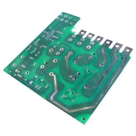
Introduction to Single-Sided PCB
A Single-Sided PCB, also known as a one-sided PCB or single-layer PCB, is a printed circuit board that has conductive copper traces on only one side of the board. This type of PCB is the simplest and most cost-effective solution for many electronic projects, especially for low-complexity circuits and prototypes.
Advantages of Single-Sided PCB
- Cost-effective: Single-sided PCBs are the most affordable option due to their simple design and manufacturing process.
- Easy to design: With only one conductive layer, single-sided PCBs are easier to design compared to multi-layer PCBs.
- Quick turnaround: The manufacturing process for single-sided PCBs is faster, allowing for shorter lead times.
- Suitable for low-complexity circuits: Single-sided PCBs are ideal for simple circuits with fewer components and connections.
Disadvantages of Single-Sided PCB
- Limited routing options: With only one conductive layer, routing complex circuits can be challenging and may require jumper wires.
- Lower component density: Single-sided PCBs have limited space for components, which can result in larger board sizes.
- Reduced electrical performance: Single-sided PCBs may have higher electromagnetic interference (EMI) and lower signal integrity compared to multi-layer PCBs.
Design Considerations for Single-Sided PCB
Component Placement
When designing a single-sided PCB, component placement is crucial to minimize the number of jumper wires and optimize the routing process. Follow these tips for effective component placement:
– Place components in a logical sequence based on the circuit schematic.
– Group related components together to reduce the distance between connections.
– Position components to minimize the number of trace crossovers.
– Consider the physical size and orientation of components to ensure proper fitting on the board.
Trace Routing
Routing traces on a single-sided PCB requires careful planning to avoid unnecessary crossovers and maintain signal integrity. Keep these guidelines in mind:
– Use wider traces for power and ground connections to reduce resistance and improve current-carrying capacity.
– Maintain appropriate trace spacing to prevent short circuits and minimize crosstalk.
– Utilize 45-degree angles for trace corners to avoid sharp bends that can cause signal reflections.
– Incorporate ground planes where possible to reduce EMI and improve signal quality.
Jumper Wires
In some cases, using jumper wires on a single-sided PCB is necessary to complete connections that cannot be routed on the copper layer. When using jumper wires:
– Keep jumper wires as short as possible to minimize signal degradation and inductance.
– Use insulated wires to prevent short circuits.
– Secure jumper wires to the board using solder or adhesive to prevent movement and ensure reliable connections.

Manufacturing Process for Single-Sided PCB
PCB Fabrication Steps
- Substrate preparation: The PCB substrate, typically made of FR-4 material, is cleaned and prepared for the copper layer.
- Copper lamination: A thin layer of copper foil is laminated onto one side of the substrate using heat and pressure.
- Photoresist application: A light-sensitive photoresist is applied to the copper layer.
- Exposure and development: The photoresist is exposed to UV light through a photomask, which hardens the exposed areas. The unexposed areas are then removed during the development process.
- Etching: The exposed copper is etched away using a chemical solution, leaving only the desired conductive traces.
- Photoresist removal: The remaining photoresist is stripped away, revealing the final copper pattern.
- Soldermask application (optional): A soldermask layer can be applied to protect the copper traces and prevent short circuits.
- Silkscreen printing (optional): A silkscreen layer can be added to label components and provide visual guidance for assembly.
- Surface finish (optional): A surface finish, such as HASL or ENIG, can be applied to protect the copper traces and improve solderability.
PCB Assembly Methods
Single-sided PCBs can be assembled using various methods, depending on the components and production volume. Common assembly methods include:
- Hand soldering: Suitable for low-volume production and prototypes, hand soldering involves manually soldering components onto the PCB using a soldering iron.
- Wave soldering: Automated process where the PCB is passed over a wave of molten solder, which solders the components to the board. Suitable for through-hole components and higher-volume production.
- Reflow soldering: Used for surface-mount components, reflow soldering involves applying solder paste to the PCB PADS, placing components, and heating the board in a reflow oven to melt the solder and form connections.

Design Software for Single-Sided PCB
There are various PCB design software options available, ranging from free, open-source tools to professional, paid solutions. Some popular choices include:
- KiCad: A free, open-source PCB design software that offers schematic capture, PCB layout, and 3D viewing capabilities.
- Eagle: A widely-used PCB design software that provides schematic capture, PCB layout, and autorouting features. Offers a free version with limitations and paid versions with advanced features.
- Altium Designer: A professional-grade PCB design software with advanced features for schematic capture, PCB layout, simulation, and manufacturing preparation.
- EasyEDA: A web-based PCB design platform that allows users to create schematics, PCB layouts, and generate Gerber files for manufacturing. Offers a free version with limitations and paid plans for additional features.

Cost-Saving Strategies for Single-Sided PCB
Optimizing PCB Design
- Minimize board size: Reducing the overall dimensions of your PCB can lower material costs and manufacturing fees.
- Use standard component sizes: Selecting components with standard footprints and sizes can reduce the need for custom manufacturing and lower costs.
- Optimize component placement: Efficient component placement can minimize the board size and reduce the number of required layers.
- Avoid unnecessary features: Eliminating non-essential features, such as complex shapes or extra silkscreen markings, can simplify manufacturing and reduce costs.
Choosing the Right Manufacturer
- Research and compare: Get quotes from multiple PCB Manufacturers to find the best balance between cost, quality, and lead time.
- Consider offshore options: Offshore PCB manufacturers, particularly those in Asia, often offer lower prices due to lower labor and material costs.
- Evaluate minimum order quantities (MOQs): Some manufacturers may offer lower prices for higher order quantities. Consider your production volume and choose a manufacturer with MOQs that align with your needs.
Ordering in Bulk
- Economy of scale: Ordering larger quantities of PCBs can result in lower per-unit costs due to the manufacturer’s ability to optimize production and distribute fixed costs across more units.
- Plan for future needs: If you anticipate ongoing production or multiple projects using the same PCB design, ordering in bulk can provide long-term cost savings.
- Consider inventory management: While bulk ordering can save money, be mindful of storage costs and the risk of holding obsolete inventory if your design changes.
Frequently Asked Questions (FAQ)
-
Q: Can single-sided PCBs be used for high-frequency circuits?
A: Single-sided PCBs are generally not recommended for high-frequency circuits due to their limited ability to control impedance and higher susceptibility to EMI. For high-frequency applications, multi-layer PCBs with proper grounding and shielding are typically required. -
Q: Are there any limitations on the number of components that can be used on a single-sided PCB?
A: The number of components that can be placed on a single-sided PCB is limited by the available board space and the ability to route traces effectively. As the number of components increases, routing becomes more challenging, and jumper wires may be necessary. In some cases, it may be more practical to transition to a double-sided or multi-layer PCB. -
Q: Can single-sided PCBs be used for surface-mount components?
A: Yes, single-sided PCBs can accommodate surface-mount components. However, the placement and routing of surface-mount components on a single-sided PCB can be more challenging compared to through-hole components due to the smaller footprints and closer spacing. -
Q: How can I ensure the reliability of single-sided PCBs?
A: To ensure the reliability of single-sided PCBs, follow best practices in design and manufacturing, such as using appropriate trace widths, maintaining proper spacing between components and traces, and selecting high-quality materials. Additionally, consider applying a soldermask and surface finish to protect the copper traces and improve solderability. -
Q: Are there any environmental concerns associated with the manufacturing of single-sided PCBs?
A: The manufacturing process for single-sided PCBs involves the use of chemicals, such as etchants and solvents, which can have environmental impacts if not properly managed. Responsible PCB manufacturers should adhere to environmental regulations and implement proper waste management and disposal practices to minimize the environmental footprint of PCB production.
Conclusion
Single-sided PCBs offer a cost-effective and efficient solution for many electronic projects, particularly those with low complexity and simple routing requirements. By understanding the design considerations, manufacturing processes, and cost-saving strategies associated with single-sided PCBs, you can optimize your PCB design and production to achieve reliable results while minimizing expenses.
When designing single-sided PCBs, prioritize component placement, trace routing, and the judicious use of jumper wires to ensure a manufacturable and functional board. Utilize PCB design software that suits your needs and budget, and consider the trade-offs between free and paid options based on your project requirements.
To maximize cost savings, optimize your PCB design by minimizing board size, using standard component sizes, and avoiding unnecessary features. Research and compare PCB manufacturers to find the best balance between cost, quality, and lead time, and consider the benefits of bulk ordering when appropriate.
By following best practices and making informed decisions throughout the design and manufacturing process, you can leverage the advantages of single-sided PCBs to create cost-effective and reliable electronic products.


Leave a Reply