Introduction to Wave soldering
Wave soldering is a widely used technique for soldering through-hole (PTH) components onto printed circuit boards (PCBs). It involves passing the PCB over a molten solder wave, which creates a reliable electrical and mechanical connection between the component leads and the PCB. Wave soldering has been a staple in the electronics manufacturing industry for decades due to its efficiency, reliability, and cost-effectiveness.
Advantages of Wave Soldering
- High throughput: Wave soldering enables the rapid soldering of multiple components simultaneously, making it suitable for high-volume production.
- Consistency: The automated nature of wave soldering ensures consistent solder joint quality across the entire PCB.
- Reliability: When properly optimized, wave soldering produces reliable solder joints that can withstand harsh environmental conditions and mechanical stresses.
- Cost-effective: Wave soldering is an economical method for soldering PTH components, especially when compared to manual soldering processes.
The Wave Soldering Process
The wave soldering process consists of several key steps that ensure the formation of high-quality solder joints. Understanding each step is crucial for optimizing the process and achieving the desired results.
1. PCB Preparation
Before wave soldering, the PCB must undergo a series of preparation steps:
a. Solder mask application: A solder mask is applied to the PCB to protect the areas that should not be soldered and to prevent solder bridges.
b. Silk screen printing: Component designators, polarity markers, and other relevant information are printed on the PCB using silk screen printing.
c. Flux application: A thin layer of flux is applied to the PCB to remove oxides, improve solder wettability, and protect the metal surfaces during soldering.
2. Component Placement
PTH components are inserted into the corresponding holes on the PCB. This process can be performed manually or using automated insertion machines, depending on the production volume and component types.
3. Preheating
The populated PCB is preheated to activate the flux and remove any remaining moisture. Preheating helps to minimize thermal shock during the soldering process and improves solder joint quality. The preheating temperature and duration are carefully controlled to avoid component damage.
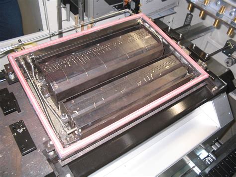
4. Wave Soldering
The preheated PCB is transported over a molten solder wave. As the board comes into contact with the wave, the molten solder flows up through the PCB holes and around the component leads, creating a strong solder joint. The solder wave is typically composed of a tin-lead alloy, although lead-free alternatives are increasingly being used to comply with environmental regulations.
5. Cooling
After passing through the solder wave, the PCB is cooled to allow the solder joints to solidify. Proper cooling is essential to prevent thermal stress and ensure the formation of strong, reliable solder joints.
6. Cleaning
Depending on the flux type used, the soldered PCB may require cleaning to remove flux residues. Cleaning can be performed using various methods, such as aqueous cleaning, solvent cleaning, or no-clean fluxes that do not require post-soldering cleaning.
7. Inspection
The soldered PCB undergoes visual inspection to identify any defects, such as solder bridges, insufficient solder, or damaged components. Automated optical inspection (AOI) systems can be employed for high-volume production to detect and classify defects quickly and accurately.

Process Parameters and Optimization
To achieve high-quality solder joints and minimize defects, several key process parameters must be carefully controlled and optimized.
Solder Alloy Selection
The choice of solder alloy is critical for wave soldering. Traditionally, tin-lead (SnPb) alloys, such as Sn63Pb37, have been widely used due to their excellent wetting properties and reliability. However, with the introduction of the Restriction of Hazardous Substances (RoHS) directive, lead-free alloys, such as Sn96.5Ag3.0Cu0.5 (SAC305), have gained popularity. Lead-free alloys have higher melting points and may require adjustments to the soldering process parameters.
Flux Selection
Flux plays a vital role in wave soldering by removing oxides, promoting solder wetting, and protecting the metal surfaces during soldering. There are several types of fluxes available, each with its own advantages and limitations:
- Rosin-based fluxes: These fluxes are derived from natural rosin and are available in various activity levels (mild, activated, and highly activated). They provide good solderability and are suitable for most applications.
- Water-soluble fluxes: These fluxes are designed to be easily removed with water after soldering. They offer excellent solderability but require thorough cleaning to prevent corrosion.
- No-clean fluxes: These fluxes leave minimal residue after soldering and do not require post-soldering cleaning. They are suitable for applications where cleaning is not feasible or desirable.
The choice of flux depends on factors such as the PCB material, component types, and environmental requirements.
Preheat Temperature and Duration
Proper preheating is essential for activating the flux, removing moisture, and preventing thermal shock during wave soldering. The preheat temperature and duration must be carefully controlled to ensure optimal results.
| PCB Type | Preheat Temperature Range | Preheat Duration |
|---|---|---|
| Single-sided | 80-100°C | 30-60 seconds |
| Double-sided | 100-120°C | 60-90 seconds |
| Multi-layer | 120-150°C | 90-120 seconds |
It is important to monitor the preheat temperature using thermocouples or infrared sensors to maintain consistency and prevent overheating, which can lead to component damage or PCB warpage.
Solder Wave Height and Velocity
The solder wave height and velocity are critical parameters that affect the quality of the solder joints. The wave height should be sufficient to ensure complete wetting of the component leads and PCB holes without causing solder bridges or excessive solder consumption. The wave velocity should be optimized to provide adequate contact time between the molten solder and the PCB while preventing solder splashes or defects.
Typical wave heights range from 1/2 to 1 inch, depending on the PCB and component dimensions. Wave velocities are usually between 0.5 to 2.0 inches per second.
Conveyor Speed and Angle
The conveyor speed and angle determine the exposure time of the PCB to the solder wave and the drainage of excess solder. Slower conveyor speeds increase the contact time between the PCB and the solder wave, allowing for better solder penetration and wetting. However, excessively slow speeds may cause solder bridges or damage to heat-sensitive components.
The conveyor angle, typically between 5 to 8 degrees, allows excess solder to drain back into the solder pot, preventing solder buildup on the PCB. It is important to optimize the conveyor speed and angle based on the specific PCB design and component types.

Defects and Troubleshooting
Despite careful process control and optimization, wave soldering defects can still occur. Identifying and addressing these defects is crucial for maintaining high product quality and reliability.
Common Wave Soldering Defects
- Solder bridges: Unintended connections between adjacent solder joints caused by excessive solder or inadequate solder mask coverage.
- Insufficient solder: Incomplete or weak solder joints resulting from inadequate solder wave height, low preheat temperature, or contaminated surfaces.
- Solder balls: Small spheres of solder that adhere to the PCB surface, often caused by excessive solder or turbulent wave flow.
- Icicles: Sharp, pointed solder formations that occur when the PCB exits the solder wave too slowly or at an incorrect angle.
- Damaged components: Components that have been damaged due to excessive heat exposure or mechanical stress during the soldering process.
Troubleshooting and Prevention
To minimize wave soldering defects, consider the following troubleshooting and prevention techniques:
- Optimize process parameters: Continuously monitor and adjust the preheat temperature, solder wave height and velocity, conveyor speed and angle, and other critical parameters to maintain consistency and prevent defects.
- Ensure proper PCB design: Collaborate with PCB designers to ensure adequate solder mask coverage, component spacing, and hole sizes to facilitate effective wave soldering.
- Maintain solder bath quality: Regularly monitor the solder bath composition and temperature to ensure consistent solder joint quality. Remove dross and contaminants as needed.
- Use appropriate fixturing: Employ well-designed fixturing to hold the PCB securely and prevent component movement during the soldering process.
- Implement quality control measures: Conduct regular visual inspections and use automated inspection systems to detect and analyze defects. Establish a feedback loop to continuously improve the soldering process based on inspection results.

Frequently Asked Questions (FAQs)
-
Q: What are the advantages of wave soldering compared to other soldering methods?
A: Wave soldering offers several advantages, including high throughput, consistency, reliability, and cost-effectiveness. It is particularly suitable for soldering through-hole components onto PCBs in high-volume production. -
Q: Can wave soldering be used for surface mount components?
A: While wave soldering is primarily used for through-hole components, it can be adapted for soldering surface mount components using a technique called Pin-in-Paste (PIP). However, for most surface mount applications, reflow soldering is the preferred method. -
Q: What is the purpose of applying flux in wave soldering?
A: Flux serves multiple purposes in wave soldering. It removes oxides from the metal surfaces, improves solder wettability, and protects the surfaces from oxidation during the soldering process. Flux selection is critical for achieving high-quality solder joints. -
Q: How can I prevent solder bridges in wave soldering?
A: To prevent solder bridges, ensure adequate solder mask coverage between adjacent pads, optimize the solder wave height and velocity, and adjust the conveyor speed and angle to allow proper drainage of excess solder. Regularly inspecting and maintaining the solder bath can also help minimize solder bridges. -
Q: What should I consider when selecting a solder alloy for wave soldering?
A: When selecting a solder alloy, consider factors such as the melting temperature, wetting properties, mechanical strength, and compatibility with the PCB and component materials. Tin-lead alloys are widely used for their excellent solderability, while lead-free alloys, such as SAC305, are becoming increasingly popular due to environmental regulations.
Conclusion
Wave soldering is a reliable and efficient method for soldering through-hole components onto PCBs. By understanding the process steps, optimizing the key parameters, and addressing common defects, manufacturers can achieve high-quality solder joints and improve product reliability. As technology advances and environmental regulations evolve, wave soldering techniques and materials will continue to adapt to meet the changing needs of the electronics industry.


Leave a Reply