What is Wave soldering?
Wave soldering is a bulk soldering process that involves passing a PCB over a wave of molten solder. The molten solder is pumped up through a nozzle, creating a wave that washes over the bottom of the PCB. The components on the PCB are then soldered to the board as the wave of solder comes into contact with the component leads and the PCB PADS.
Wave soldering is typically used for through-hole components, which have leads that pass through holes in the PCB. However, it can also be used for surface-mount components with the use of additional fixtures and pallets.
History of Wave Soldering
Wave soldering was first introduced in the 1950s as a way to automate the soldering process for PCBs. Prior to wave soldering, soldering was done manually, which was a time-consuming and labor-intensive process. Wave soldering allowed for much faster and more efficient soldering of PCBs, which helped to drive down the cost of electronics manufacturing.
Over the years, wave soldering technology has continued to evolve and improve. Today, wave soldering machines are highly automated and can handle a wide range of PCB sizes and component types.

How Wave Soldering Works
The wave soldering process involves several steps:
-
PCB Preparation: The PCB is first cleaned and inspected to ensure that it is free of contaminants and defects. The components are then inserted into the PCB, either manually or using automated pick-and-place machines.
-
Fluxing: The PCB is then passed through a fluxing station, where a thin layer of flux is applied to the bottom of the board. Flux is a chemical that helps to clean the metal surfaces and promote better solder wetting.
-
Preheating: The PCB is then passed through a preheating zone, where it is heated to a temperature just below the melting point of the solder. This helps to activate the flux and prepare the board for soldering.
-
Wave Soldering: The PCB is then passed over the wave of molten solder. The solder wave is typically created by pumping the molten solder up through a nozzle. As the PCB passes over the wave, the molten solder washes over the bottom of the board, soldering the component leads to the PCB pads.
-
Cooling: After passing over the solder wave, the PCB is then cooled to allow the solder to solidify. This is typically done using air knives or fans.
-
Cleaning: Finally, the PCB is cleaned to remove any excess flux or solder residue.

Types of Wave Soldering
There are two main types of wave soldering: single wave and dual wave.
Single Wave Soldering
Single wave soldering uses a single wave of molten solder to solder the components to the PCB. The wave is typically turbulent, which helps to ensure good solder coverage and wetting. Single wave soldering is typically used for simpler PCBs with fewer components.
Dual Wave Soldering
Dual wave soldering uses two waves of molten solder: a turbulent wave followed by a laminar wave. The turbulent wave helps to ensure good solder coverage and wetting, while the laminar wave helps to remove excess solder and create a smooth, even solder joint. Dual wave soldering is typically used for more complex PCBs with a higher density of components.

Advantages of Wave Soldering
Wave soldering offers several advantages over other Soldering Methods:
-
Speed: Wave soldering is a highly automated process that can solder a large number of PCBs in a short amount of time. This makes it ideal for high-volume production runs.
-
Consistency: Wave soldering produces consistent, high-quality solder joints across the entire PCB. This helps to reduce the risk of defects and improve the overall reliability of the finished product.
-
Cost-effective: Wave soldering is a cost-effective method for soldering PCBs, particularly for high-volume production runs. The automation of the process helps to reduce labor costs and improve efficiency.
-
Versatility: Wave soldering can be used for a wide range of PCB sizes and component types, making it a versatile soldering method.
Disadvantages of Wave Soldering
While wave soldering offers many advantages, there are also some disadvantages to consider:
-
Limited component types: Wave soldering is primarily used for through-hole components and may not be suitable for certain types of surface-mount components.
-
Thermal shock: The high temperatures used in wave soldering can cause thermal shock to some components, which can lead to damage or failure.
-
Solder bridges: If the solder wave is not properly controlled, it can cause solder bridges between adjacent pads or components.
-
Flux residue: The use of flux in wave soldering can leave residue on the PCB, which may require additional cleaning steps.
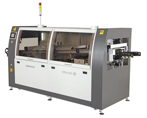
Wave Soldering Equipment
Wave soldering requires specialized equipment to create the molten solder wave and control the soldering process. The main components of a wave soldering machine include:
-
Solder pot: The solder pot holds the molten solder and is typically made of a material that can withstand high temperatures, such as titanium or ceramic.
-
Solder pump: The solder pump is used to pump the molten solder up through the nozzle to create the solder wave.
-
Nozzle: The nozzle is used to shape the solder wave and control the flow of solder over the PCB.
-
Conveyor: The conveyor is used to transport the PCB through the various stages of the wave soldering process, including fluxing, preheating, and soldering.
-
Preheater: The preheater is used to heat the PCB to the appropriate temperature before it enters the solder wave.
-
Cooling system: The cooling system is used to cool the PCB after it has passed through the solder wave to allow the solder to solidify.
Wave Soldering Process Parameters
To ensure a successful wave soldering process, several key parameters must be carefully controlled:
-
Solder temperature: The temperature of the molten solder must be carefully controlled to ensure proper wetting and solder joint formation. The ideal temperature range depends on the type of solder being used but is typically between 240-260°C.
-
Conveyor speed: The speed of the conveyor must be carefully controlled to ensure that the PCB spends the appropriate amount of time in each stage of the process. If the conveyor speed is too fast, the PCB may not be properly heated or cooled, while if it is too slow, the PCB may be exposed to the solder wave for too long, causing damage or defects.
-
Preheat temperature: The preheat temperature must be carefully controlled to ensure that the PCB is heated to the appropriate temperature before entering the solder wave. The ideal preheat temperature depends on the type of PCB and components being used but is typically between 80-120°C.
-
Flux type and application: The type and amount of flux used must be carefully controlled to ensure proper cleaning and wetting of the metal surfaces. Too little flux can result in poor solder joint formation, while too much flux can leave residue on the PCB.
-
Nozzle design: The design of the solder nozzle must be carefully chosen to ensure the appropriate shape and flow of the solder wave. The nozzle design can affect the speed and direction of the solder flow, as well as the amount of turbulence in the wave.
Common Defects in Wave Soldering
Despite careful control of the wave soldering process parameters, defects can still occur. Some common defects include:
-
Solder bridges: Solder bridges occur when solder flows between adjacent pads or components, creating an unintended electrical connection. Solder bridges can be caused by excessive solder, improper nozzle design, or incorrect conveyor speed.
-
Incomplete solder joints: Incomplete solder joints occur when the solder does not completely fill the hole or cover the pad, resulting in a weak or unreliable connection. Incomplete solder joints can be caused by insufficient solder, poor wetting, or incorrect preheat temperature.
-
Lifted components: Lifted components occur when the component leads are not properly soldered to the PCB, causing the component to lift away from the board. Lifted components can be caused by insufficient solder, poor wetting, or thermal shock.
-
Solder balls: Solder balls are small spheres of solder that can form on the PCB or components during the soldering process. Solder balls can be caused by excessive solder, improper nozzle design, or incorrect conveyor speed.
Troubleshooting Wave Soldering Defects
If defects are detected during the wave soldering process, several steps can be taken to troubleshoot and correct the problem:
-
Check process parameters: The first step in troubleshooting wave soldering defects is to check the process parameters, including solder temperature, conveyor speed, preheat temperature, and flux application. Ensure that all parameters are within the appropriate range for the PCB and components being used.
-
Inspect nozzle design: Inspect the solder nozzle to ensure that it is the appropriate design for the PCB and components being used. A poorly designed nozzle can cause turbulence in the solder wave, leading to defects such as solder bridges or incomplete solder joints.
-
Adjust solder level: Ensure that the solder level in the pot is appropriate for the PCB being soldered. Too little solder can result in incomplete solder joints, while too much solder can cause solder bridges or solder balls.
-
Check component placement: Ensure that all components are properly placed on the PCB and that the leads are properly inserted through the holes. Improperly placed components can cause lifted components or incomplete solder joints.
-
Adjust fluxing: Ensure that the appropriate type and amount of flux is being applied to the PCB. Too little flux can result in poor wetting and incomplete solder joints, while too much flux can leave residue on the PCB.
Alternatives to Wave Soldering
While wave soldering is a widely used and effective method for soldering PCBs, there are several alternatives that may be more appropriate for certain applications:
-
Reflow soldering: Reflow soldering is a process that involves applying solder paste to the PCB pads and then heating the entire board to melt the solder and create the solder joints. Reflow soldering is typically used for surface-mount components and can produce high-quality solder joints with minimal defects.
-
Selective soldering: Selective soldering is a process that involves applying solder to specific areas of the PCB using a mini-wave or laser. Selective soldering is typically used for PCBs with a mix of through-hole and surface-mount components and can provide more precise control over the soldering process.
-
Hand soldering: Hand soldering is a manual process that involves applying solder to each component lead and pad individually using a soldering iron. Hand soldering is typically used for low-volume production runs or prototypes and can provide more flexibility and control over the soldering process.
Conclusion
Wave soldering is a highly automated and efficient method for soldering PCBs that has been widely used in the electronics industry for decades. By carefully controlling the process parameters and using specialized equipment, wave soldering can produce high-quality solder joints with minimal defects.
However, wave soldering does have some limitations and may not be suitable for all applications. Alternative methods such as reflow soldering, selective soldering, and hand soldering may be more appropriate in certain situations.
Overall, wave soldering remains an important tool in the electronics manufacturing process and will likely continue to be used for many years to come.
FAQ
-
What is the difference between single wave and dual wave soldering?
Single wave soldering uses a single wave of molten solder to solder the components to the PCB, while dual wave soldering uses two waves: a turbulent wave followed by a laminar wave. Dual wave soldering is typically used for more complex PCBs with a higher density of components. -
Can wave soldering be used for surface-mount components?
Yes, wave soldering can be used for surface-mount components, but it may require additional fixtures and pallets to hold the components in place during the soldering process. Reflow soldering is typically a more appropriate method for soldering surface-mount components. -
What is the purpose of flux in wave soldering?
Flux is a chemical that is applied to the PCB before soldering to clean the metal surfaces and promote better solder wetting. Flux helps to remove oxides and other contaminants from the metal surfaces, allowing the solder to flow more easily and create a stronger bond. -
What is the ideal temperature range for wave soldering?
The ideal temperature range for wave soldering depends on the type of solder being used but is typically between 240-260°C. The temperature must be carefully controlled to ensure proper wetting and solder joint formation. -
How can wave soldering defects be prevented?
Wave soldering defects can be prevented by carefully controlling the process parameters, including solder temperature, conveyor speed, preheat temperature, flux application, and nozzle design. Proper maintenance and calibration of the wave soldering equipment can also help to prevent defects. If defects do occur, troubleshooting steps such as checking process parameters, inspecting nozzle design, adjusting solder level, checking component placement, and adjusting fluxing can help to identify and correct the problem.


Leave a Reply