Introduction to PCB Stencils
PCB stencils are an essential tool in the electronics manufacturing process, allowing for precise and efficient application of solder paste to printed circuit boards (PCBs). These stencils are typically made from durable materials such as stainless steel or polyimide and feature apertures that correspond to the pads on the PCB where components will be placed.
The Role of PCB Stencils in Electronics Manufacturing
PCB stencils play a crucial role in the surface mount technology (SMT) assembly process. They ensure that the correct amount of solder paste is deposited onto the PCB Pads, which is essential for creating reliable solder joints between components and the board. The use of stencils helps to minimize defects such as bridging, insufficient solder, or solder balls, leading to higher quality assemblies and reduced rework costs.
Types of PCB Stencils
There are several types of PCB stencils available, each with its own advantages and applications:
-
Stainless Steel Stencils: These are the most common type of PCB stencils, offering durability, precision, and compatibility with a wide range of solder pastes. Stainless steel stencils are suitable for high-volume production and can be easily cleaned and reused.
-
Polyimide Stencils: Also known as polymer stencils, these are made from a flexible, high-temperature resistant material. Polyimide stencils are ideal for applications requiring fine pitch components or intricate patterns, as they can conform to slight variations in PCB topography.
-
Electroformed Stencils: These stencils are created using an electroplating process, resulting in highly precise apertures with smooth walls. Electroformed stencils are suitable for applications requiring very fine features or tight tolerances, such as micro-BGA or flip-chip packaging.
-
Step Stencils: These stencils feature multiple levels or steps, allowing for different solder paste deposit heights on the same PCB. Step stencils are useful for applications with components of varying heights or when different solder paste volumes are required for specific components.
Designing PCB Stencils
Aperture Design Considerations
When designing PCB stencils, several factors must be considered to ensure optimal solder paste deposition and assembly quality:
-
Aperture Size: The size of the stencil apertures should be based on the dimensions of the PCB pads and the type of components being used. As a general rule, the aperture size should be slightly larger than the pad size to allow for proper solder paste release.
-
Aperture Shape: The shape of the apertures can affect solder paste release and the resulting Solder Joint Quality. Common aperture shapes include square, rectangular, and circular. The choice of aperture shape depends on factors such as pad geometry, component type, and solder paste properties.
-
Aperture Orientation: The orientation of the apertures relative to the PCB pads can impact solder paste deposition and component placement accuracy. Apertures should be aligned with the pads to ensure proper solder paste transfer and minimize the risk of bridging or insufficent solder.
-
Aperture Pitch: The pitch, or spacing between apertures, must be carefully considered to avoid solder paste bridging between adjacent pads. The minimum pitch is determined by factors such as the solder paste particle size, stencil thickness, and printing parameters.
Stencil Thickness Selection
The thickness of a PCB stencil directly affects the volume of solder paste deposited onto the PCB pads. Selecting the appropriate stencil thickness is crucial for achieving the desired solder joint quality and reliability. Factors to consider when choosing stencil thickness include:
-
Component Type and Size: Smaller components, such as chip resistors or capacitors, require thinner stencils to prevent excessive solder paste deposition, which can lead to bridging or tombstoning. Larger components, such as QFPs or BGAs, may require thicker stencils to ensure sufficient solder paste volume for proper wetting and joint formation.
-
PCB Pad Size and Pitch: The size and spacing of the PCB pads also influence stencil thickness selection. Fine-pitch components and smaller pads generally require thinner stencils to maintain proper paste release and prevent bridging.
-
Solder Paste Properties: The rheological properties of the solder paste, such as viscosity and particle size, should be considered when selecting stencil thickness. Thicker pastes or those with larger particle sizes may require thicker stencils to ensure adequate paste release and volume.
| Component Type | Typical Stencil Thickness |
|---|---|
| Chip Components (0201-0603) | 0.1 mm – 0.15 mm |
| Chip Components (0805-1206) | 0.125 mm – 0.2 mm |
| SOICs, QFPs | 0.125 mm – 0.15 mm |
| BGAs, CSPs | 0.125 mm – 0.15 mm |
| Large Connectors, Power Components | 0.15 mm – 0.2 mm |
Note: These values are general guidelines and may vary depending on specific application requirements and solder paste properties.
Stencil Material Selection
The choice of stencil material depends on factors such as durability, precision, and compatibility with the solder paste and cleaning processes. The most common stencil materials are stainless steel and polyimide.
-
Stainless Steel: Stainless steel stencils offer excellent durability, precision, and compatibility with a wide range of solder pastes. They are suitable for high-volume production and can withstand repeated cleaning cycles. However, stainless steel stencils may be more prone to wear and damage compared to polyimide stencils.
-
Polyimide: Polyimide stencils are made from a flexible, high-temperature resistant polymer material. They offer several advantages over stainless steel stencils, including improved conformability to PCB topography, reduced risk of damage to the PCB or components during printing, and compatibility with finer pitch components and intricate patterns. However, polyimide stencils may have a shorter lifespan than stainless steel stencils and require more frequent replacement.
| Material | Advantages | Disadvantages |
|---|---|---|
| Stainless Steel | – Durable – Precise – Compatible with most solder pastes – Suitable for high-volume production |
– Prone to wear and damage – May damage PCBs or components during printing – Less suitable for fine-pitch components |
| Polyimide | – Conforms to PCB topography – Reduced risk of PCB/component damage – Suitable for fine-pitch components and intricate patterns |
– Shorter lifespan compared to stainless steel – Requires more frequent replacement – May not be compatible with all solder pastes |

PCB Stencil Manufacturing Process
Chemical Etching
Chemical etching is the most common method for manufacturing PCB stencils. The process involves the following steps:
-
Photoresist Application: A light-sensitive photoresist layer is applied to both sides of the stencil material.
-
Exposure: The photoresist is exposed to UV light through a photomask, which contains the desired stencil pattern. The UV light hardens the exposed areas of the photoresist.
-
Developing: The unexposed areas of the photoresist are removed using a chemical developer, leaving the stencil pattern protected by the hardened photoresist.
-
Etching: The stencil material is immersed in an etching solution, which removes the unprotected areas, creating the apertures in the stencil.
-
Stripping: The remaining photoresist is stripped away, leaving the finished stencil.
Chemical etching offers a cost-effective solution for producing high-quality PCB stencils with precise apertures and smooth walls.
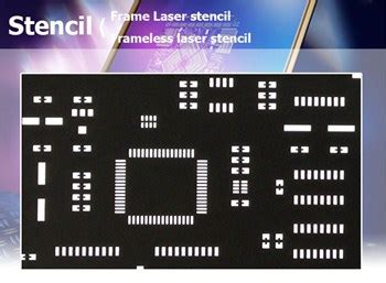
Laser Cutting
Laser cutting is an alternative method for manufacturing PCB stencils, particularly for applications requiring very fine features or rapid prototyping. The process uses a high-powered laser to vaporize the stencil material in the desired pattern, creating the apertures.
Laser cutting offers several advantages over chemical etching:
-
Faster Turnaround: Laser cutting eliminates the need for photoresist application, exposure, and developing, resulting in faster stencil production times.
-
Finer Features: Laser cutting can produce apertures with smaller dimensions and tighter tolerances compared to chemical etching.
-
No Chemical Waste: Laser cutting is an environmentally friendly process that does not generate chemical waste.
However, Laser-Cut Stencils may have slightly rougher aperture walls compared to chemically etched stencils, which can affect solder paste release and print quality.

PCB Stencil Inspection and Quality Control
To ensure the highest quality PCB stencils, several inspection and quality control measures are employed during the manufacturing process:
-
Visual Inspection: Stencils are visually inspected for defects such as misaligned apertures, incomplete etching, or damage to the stencil material.
-
Dimensional Verification: The aperture dimensions and positions are verified using optical or laser-based measurement systems to ensure they meet the specified tolerances.
-
Thickness Measurement: Stencil thickness is measured at multiple points to ensure uniformity and compliance with the specified thickness.
-
Cleaning and Packaging: Stencils are thoroughly cleaned to remove any debris or contaminants and are packaged in protective materials to prevent damage during shipping and storage.
Regular quality control checks and inspections throughout the manufacturing process help to identify and correct any issues, ensuring that the final stencils meet the highest standards of precision and reliability.

Frequently Asked Questions (FAQ)
-
What is the typical lifespan of a PCB stencil?
The lifespan of a PCB stencil depends on various factors, such as the stencil material, printing volume, and cleaning frequency. Stainless steel stencils can last for thousands of prints with proper care and maintenance, while polyimide stencils may need to be replaced more frequently. Regular inspection and cleaning can help extend the lifespan of a stencil. -
How often should PCB stencils be cleaned?
PCB stencils should be cleaned regularly to remove solder paste residue and prevent contamination of the printing process. The frequency of cleaning depends on the printing volume and the type of solder paste used. As a general guideline, stencils should be cleaned every 4-8 hours of continuous printing or between shifts. More frequent cleaning may be necessary for high-volume production or when using no-clean solder pastes. -
Can damaged PCB stencils be repaired?
In some cases, minor damage to PCB stencils can be repaired using specialized techniques such as laser welding or chemical filling. However, the feasibility and effectiveness of repair depend on the extent and location of the damage. For significant damage or wear, it is often more cost-effective to replace the stencil rather than attempting a repair. -
How should PCB stencils be stored when not in use?
PCB stencils should be stored in a clean, dry environment to prevent damage and contamination. Stencils should be placed in protective packaging, such as plastic bags or containers, to minimize exposure to dust and moisture. Stencils should also be stored flat to prevent warping or deformation. Proper storage helps to maintain stencil quality and extend its lifespan. -
Can PCB stencils be customized for specific applications?
Yes, PCB stencils can be customized to meet specific application requirements. Customization options include aperture size and shape, stencil thickness, and material selection. Stencil manufacturers can work closely with customers to design and produce stencils that are optimized for their unique PCB designs and assembly processes. Customized stencils can help improve solder paste deposition accuracy and consistency, leading to higher quality assemblies and reduced defects.
Conclusion
PCB stencils are a critical component in the electronics manufacturing process, enabling precise and efficient solder paste deposition for surface mount assembly. Careful consideration of aperture design, stencil thickness, and material selection is essential for ensuring optimal solder joint quality and reliability.
Advanced PCB stencil manufacturing techniques, such as chemical etching and laser cutting, allow for the production of high-quality stencils with fine features and tight tolerances. Rigorous inspection and quality control measures throughout the manufacturing process help to maintain the highest standards of precision and consistency.
As electronics continue to miniaturize and become more complex, the demand for advanced PCB stencil solutions will only increase. By staying at the forefront of stencil technology and manufacturing processes, PCB Assembly providers can meet the evolving needs of their customers and deliver high-quality, reliable electronic assemblies.


Leave a Reply