A thermal jumper SMD component is a small, metallized aluminum nitride (AlN) pad soldered between a heat-generating device and a copper ground plane on a PCB. It provides a low-resistance thermal path — typically 170–200 W/mK through the AlN body — without any electrical connection, functioning purely as a surface-mount heat spreader. For engineers evaluating thermal jumper SMD solutions, the key advantage over alumina alternatives is a 6–8× improvement in bulk thermal conductivity.
Key Takeaways
- AlN thermal jumper SMD pads deliver 170–200 W/mK bulk thermal conductivity, roughly 6–8× higher than 96% alumina alternatives (24–28 W/mK).
- Standard sizes range from 2 mm × 2 mm to 10 mm × 10 mm, with thicknesses of 0.25–1.0 mm.
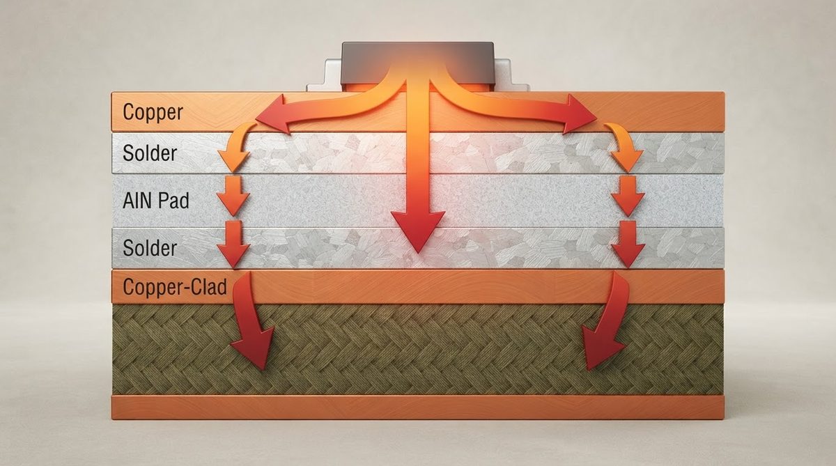
- Solder attachment (SAC305 or AuSn) creates a complete thermal path from die to ground copper in a single reflow step.
- Thermal jumpers suit applications where thermal vias alone cannot move enough heat, or where electrical isolation between planes is required.
- For heat loads above roughly 10 W in a 10 mm × 10 mm footprint, a DBC or AMB substrate is usually a better structural choice.
What a Thermal Jumper SMD Pad Actually Does
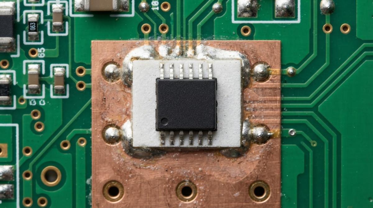
Power semiconductors, laser diodes, and RF amplifiers generate concentrated heat at their die-attach pads. A standard FR-4 board conducts only about 0.3 W/mK through its laminate, so designers use thermal vias, metal-core layers, or exposed copper pads to move heat downward. A thermal jumper SMD part adds another option: a discrete ceramic component, pick-and-placed and reflowed like any other surface-mount device, that bridges the gap between a hot pad and a thermally grounded copper area.
The jumper is electrically insulating (volume resistivity >10¹⁴ Ω·cm for AlN per Kyocera datasheet SH-15) but thermally conductive. This matters in designs where the heat-source pad sits at a different potential than the ground plane beneath it. A copper slug or metal bridge would short those nets. The AlN jumper does not.
Why AlN Instead of Alumina for a Thermal Jumper SMD Application
Alumina (96% Al₂O₃) is the default ceramic substrate material and costs roughly one-third as much as AlN per unit area. But for a thermal jumper, the entire point is minimising thermal resistance through a small, thin body. The table below shows why AlN wins in this specific application.
| Parameter | AlN | 96% Al₂O₃ | Unit | Condition | Source |
|---|---|---|---|---|---|
| Thermal conductivity | 170–200 | 24–28 | W/mK | 20 °C | Kyocera SH-15 / CoorsTek ADS-996 |
| CTE | 4.5–4.7 | 6.5–7.0 | ppm/°C | 20–300 °C | Maruwa AN series / CoorsTek |
| Dielectric strength | 14–17 | 10–15 | kV/mm | AC, 60 Hz | CeramTec Rubalit |
| Flexural strength | 300–350 | 300–380 | MPa | ASTM C1161 | CoorsTek |
| Volume resistivity | >10¹⁴ | >10¹⁴ | Ω·cm | 25 °C | Kyocera / CoorsTek |
Typical values for commercially available material, for comparison only. Confirm against the datasheet for your specific grade.
The 6–8× thermal conductivity advantage of AlN means a 0.5 mm-thick jumper produces roughly one-sixth the thermal resistance of the same-size alumina piece. For a 5 mm × 5 mm × 0.5 mm jumper carrying 3 W, the difference is meaningful: about 0.1 °C/W through AlN versus 0.7 °C/W through alumina. Details on AlN thermal conductivity and its measurement are covered separately.
Worked Example: Thermal Resistance of a 5 × 5 mm Thermal Jumper SMD Pad
Assume a 5 mm × 5 mm × 0.5 mm AlN thermal jumper (k = 180 W/mK) with SAC305 solder joints on both faces (k ≈ 58 W/mK, bondline 50 µm each side).
Through the AlN body:
R_AlN = t / (k × A) = 0.0005 / (180 × 0.000025) = 0.111 °C/W
Through each solder layer:
R_solder = 0.00005 / (58 × 0.000025) = 0.0345 °C/W
Total jumper stack:
R_total = 0.111 + 2 × 0.0345 ≈ 0.18 °C/W
At 3 W dissipation, the temperature drop across the jumper is about 0.54 °C. Compare that to the same geometry in 96% alumina (k = 26 W/mK): R_alumina body alone is 0.77 °C/W, giving a 2.5 °C drop through the body plus solder layers. For designs chasing single-digit junction-to-board temperature budgets, that 2 °C saving justifies the AlN cost premium. A deeper walkthrough of these calculations appears in the AlN thermal design guide.
Enter your own jumper dimensions, material, and power dissipation below to estimate the thermal resistance of your specific thermal jumper SMD stack.
Metallization and Soldering
A bare AlN ceramic cannot be soldered. The jumper must be metallized on both faces — typically with a Ti/Pt/Au or Ti/Ni/Au thin-film stack, or a thick-film tungsten/nickel/gold system. The metallization serves two purposes: it wets to solder, and it protects the AlN surface from hydrolysis (AlN reacts slowly with moisture if left uncoated).
Standard lead-free SAC305 reflow (peak 245–250 °C) works for most applications. For high-reliability or high-temperature environments (automotive SiC inverters, for instance), AuSn (80/20) solder reflowed at 320 °C provides better creep resistance and a higher remelt point. Choose the solder to match the rest of your assembly process; the AlN jumper itself tolerates either profile without damage.
Pad design on the host PCB follows normal SMD rules. Use solder-mask-defined pads to control fillet size. A 0.15 mm solder-mask pullback on each side is typical. Ensure the ground-plane copper beneath the jumper landing pad has adequate thermal via stitching to carry heat into the board’s thermal ground.
Common Sizes and How to Specify
Thermal jumper SMD parts are not standardised the way resistors or capacitors are. Most are custom-cut from metallized AlN wafers. Typical dimensions:
- Length × Width: 2 × 2 mm up to 10 × 10 mm. Rectangular shapes (e.g., 3 × 5 mm) are common where the heat source footprint is not square.
- Thickness: 0.25 mm, 0.38 mm, 0.5 mm, 0.635 mm, or 1.0 mm. Thinner is thermally better but mechanically more fragile during pick-and-place.
- Metallization: Specify top and bottom face coverage, metal stack, and minimum gold thickness (typically ≥ 0.5 µm for solderability).
If your design needs metallized ceramic substrates in non-standard shapes or with patterned metallization, those are manufactured with the same processes used for thermal jumpers — just at larger panel scale.
When NOT to Use an AlN Thermal Jumper SMD Part
Low heat flux, cost-sensitive designs. If the component dissipates under 0.5 W and board-level thermal vias provide adequate cooling, an AlN jumper adds cost and a placement step for marginal benefit. A field of 0.3 mm thermal vias on 1.0 mm pitch in standard FR-4 may be sufficient.
Very high power (>10 W per device). At this level, a discrete jumper on an FR-4 host board creates a thermal bottleneck at the board-level interface. A DBC or AMB power substrate — where the copper and ceramic are bonded across the full module footprint — is structurally and thermally superior.
No electrical isolation needed. If the heat-source pad and the ground plane share the same net, a copper coin or embedded copper slug does the job at lower cost and with even better thermal conductivity (390 W/mK).
Extreme vibration. Ceramic is brittle. In environments with sustained high-g vibration (e.g., some aerospace or downhole applications), a solder-attached ceramic part can crack at stress concentrations. Evaluate thermal shock and mechanical cycling test data before committing.
Frequently Asked Questions
Can I reflow an AlN thermal jumper with standard SMD components?
Yes. A metallized AlN thermal jumper solders in a standard SAC305 reflow profile (peak 245–250 °C). Place it on the board with a pick-and-place machine like any other SMD part. No special flux or atmosphere is required for standard profiles.
Does the AlN jumper need an underfill?
Not for thermal performance alone. Underfill is sometimes added in high-reliability assemblies to reduce solder joint fatigue during thermal cycling, but it slightly increases the total thermal resistance of the stack. Evaluate based on your reliability requirements, not thermal ones.
What is the maximum operating temperature of an AlN thermal jumper?
The AlN ceramic body itself is stable well above 1 000 °C in inert atmosphere. The practical limit is set by the metallization and solder. With AuSn solder, continuous operation up to about 300 °C is feasible. With SAC305, stay below 150 °C at the joint. More on AlN at high temperature is available separately.
How does a thermal jumper compare to thermal interface material (TIM)?
A TIM pad (e.g., graphite or silicone sheet) typically conducts 5–15 W/mK and compresses to fill gaps. An AlN thermal jumper SMD pad conducts 170–200 W/mK but requires solder bonds on both faces. The jumper wins on raw thermal resistance but needs a solderable interface; TIM wins on ease of assembly and tolerance to surface flatness.
Are there off-the-shelf AlN thermal jumpers I can order?
A few suppliers stock common sizes (5 × 5 mm, 10 × 10 mm) with standard Ti/Ni/Au metallization. Most thermal jumpers, however, are custom-cut to match specific die and pad geometries. Lead times for custom parts are typically 2–4 weeks for prototypes.
Next Step
If you have a specific footprint and heat load, the fastest path to a solution is to send your pad dimensions and target thermal resistance. AlN thermal jumper SMD pads are manufactured from the same high thermal conductivity substrate materials used for full ceramic PCBs, and quoting follows the same process — upload your drawing or Gerber at aluminapcb.com/instant-quote.