The most common ceramic substrate standard sizes are 2″×2″ (50.8 × 50.8 mm), 3″×3″ (76.2 × 76.2 mm), and 4.5″×4.5″ (114.3 × 114.3 mm), with thicknesses from 0.25 mm to 1.0 mm. These dimensions are carried as stock by most alumina suppliers and offer the shortest lead times. Anything outside these formats is readily produced as a custom cut, but expect longer delivery and higher per-piece cost.
Why Do “Standard” Sizes Exist for Ceramic Substrates?
Ceramic substrates are sintered from pressed powder in large batches. Kilns, lapping machines, and thick-film screen printers are tooled around a limited set of panel formats. Standardizing on a few sizes keeps tooling costs low, allows suppliers to maintain stock, and lets thick-film printers reuse screens across customers. The dominant sizes trace back to legacy inch-based tooling from the U.S. hybrid-circuit industry of the 1970s and 1980s, which is why even metric-native suppliers still list dimensions in inches.
If your final part is smaller than a stock panel, you order the nearest larger standard size and singulate after metallization using laser scribing for ceramic breakout. This panelized approach is almost always cheaper than ordering pre-cut individual pieces.
Common Stock Sizes — Reference Table
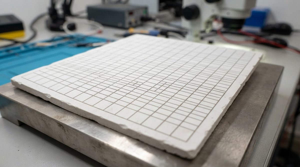
The table below lists the sizes most frequently stocked by alumina substrate manufacturers such as CoorsTek (ADS-996), Kyocera, and Maruwa. AlN and Si₃N₄ substrates share some of these formats but have a narrower selection; check the specific material datasheet.
| Size (inches) | Size (mm) | Typical thicknesses (mm) | Common material |
|---|---|---|---|
| 1″ × 1″ | 25.4 × 25.4 | 0.25, 0.38, 0.50, 0.635 | Al₂O₃ 96%, Al₂O₃ 99.6% |
| 1″ × 2″ | 25.4 × 50.8 | 0.25, 0.38, 0.50, 0.635 | Al₂O₃ 96% |
| 2″ × 2″ | 50.8 × 50.8 | 0.25, 0.38, 0.50, 0.635, 1.0 | Al₂O₃ 96%, Al₂O₃ 99.6%, AlN |
| 3″ × 3″ | 76.2 × 76.2 | 0.38, 0.50, 0.635, 1.0 | Al₂O₃ 96%, Al₂O₃ 99.6% |
| 4″ × 4″ | 101.6 × 101.6 | 0.38, 0.50, 0.635, 1.0 | Al₂O₃ 96% |
| 4.5″ × 4.5″ | 114.3 × 114.3 | 0.38, 0.50, 0.635, 1.0 | Al₂O₃ 96%, Al₂O₃ 99.6% |
| 2″ × 3″ | 50.8 × 76.2 | 0.25, 0.38, 0.635 | Al₂O₃ 96% |
Typical stock formats from major suppliers (CoorsTek, Kyocera, Maruwa). Confirm availability and dimensional tolerances against the datasheet for your specific grade.
For a full breakdown of available thickness options, see the ceramic substrate thickness chart.
How to Choose the Right Panel Size for Your Design
Start from your final singulated part size, then work outward. The goal is to fit the maximum number of parts on the smallest standard panel that your screen printer or metallization house can handle.
Worked Example: Fitting a 10 × 15 mm Part on a Panel
Suppose your finished substrate is 10 × 15 mm and you need 500 pieces. A 2″ × 2″ panel (50.8 × 50.8 mm) gives you roughly 4 columns × 3 rows = 12 parts per panel, assuming 0.3 mm scribe streets between parts and a 1.5 mm border. You would need ⌈500 / 12⌉ = 42 panels. A 4.5″ × 4.5″ panel (114.3 × 114.3 mm) fits about 10 × 7 = 70 parts, so only 8 panels — far fewer screen setups and less handling. But if your metallization house charges a higher screen fee for the larger format, the break-even point may favor the 2″ × 2″ panel at low volumes.
Key factors in the panel-size decision:
- Screen printer bed size. Most thick-film printers accept up to 4.5″ × 4.5″. Larger panels (6″ × 6″ or custom) need a bigger printer or a DPC process.
- Yield per panel. More parts per panel means fewer firings and lower unit cost.
- Warpage risk. Thinner substrates (≤ 0.25 mm) in large formats are more prone to warpage during firing. A 4.5″ × 4.5″ panel at 0.25 mm thick requires careful handling.
- Scribe street width. Laser scribe streets typically consume 0.2–0.4 mm per cut. Factor this into your nesting calculation.
Metric vs. Inch Sizes — Does It Matter?
Some Asian suppliers stock metric-native sizes such as 50 × 50 mm, 60 × 48 mm, or 100 × 100 mm. These are functionally equivalent to their inch-based counterparts for most applications. The difference between a 2″ × 2″ panel (50.8 × 50.8 mm) and a 50 × 50 mm panel is 0.8 mm per edge — enough to lose one row of parts if your nesting is tight. Always confirm the exact panel dimension in millimeters, not just the nominal inch callout.
When Custom Sizes Make Sense
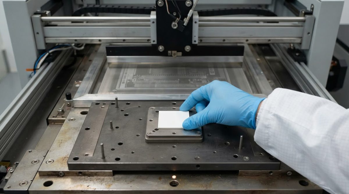
Stock sizes cover the majority of thick-film hybrid and power-module applications. Custom panel sizes are justified when:
- Your part is large enough that standard panels waste more than 30% of the substrate area.
- You need a non-rectangular shape (circular, notched, or with internal cutouts) — see custom-shape laser-cut ceramic substrates.
- Your volume is high enough (typically >5,000 panels/year) to amortize custom lapping and firing fixtures.
For prototyping or low-volume runs, stick with blank as-fired ceramic substrates in standard formats and singulate to your final dimensions.
When Not to Use a Ceramic Substrate at All
If your circuit fits on a standard FR-4 or metal-core PCB and operates below 150 °C with modest power density, ceramic is overkill. The cost premium — typically 5–15× per unit area compared to FR-4 — is only justified when you need high thermal conductivity (>20 W/mK), operation above 300 °C, tight CTE matching to GaN or SiC die, or low dielectric loss at microwave frequencies. A 100 × 100 mm single-layer FR-4 board costs under $1 in volume; the same area in 96% alumina starts around $8–$15 depending on thickness and finish.
Frequently Asked Questions
What is the largest standard ceramic substrate you can buy?
The largest commonly stocked size is 4.5″ × 4.5″ (114.3 × 114.3 mm) in 96% alumina. Some suppliers offer 6″ × 6″ panels, but these are typically made to order with a 4–6 week lead time. AlN substrates rarely exceed 2″ × 2″ as a stock item.
Can I order ceramic substrates in non-square shapes?
Yes. Substrates can be laser-cut or diamond-scribed into circles, rectangles, and complex profiles. You pay for the stock panel plus the cutting operation, so the per-piece cost is higher than a simple scribe-and-snap from a standard panel.
Do ceramic substrate sizes follow an IPC standard?
There is no IPC standard that mandates specific ceramic substrate panel sizes. The common sizes (1″, 2″, 3″, 4.5″ squares) are de facto industry standards inherited from the U.S. hybrid microelectronics industry and maintained by supplier convention.
How tight are the dimensional tolerances on a standard panel?
As-fired alumina substrates typically hold ±0.5% of the nominal dimension, per ASTM C1161 measurement practice. A 50.8 mm panel can be 50.55–51.05 mm. Lapped or laser-cut substrates tighten this to ±0.05–0.10 mm. Always specify your tolerance requirement when ordering.
Is a 2″ × 2″ AlN substrate the same price as a 2″ × 2″ alumina substrate?
No. Aluminum nitride substrates cost roughly 3–5× more than 96% alumina in the same size and thickness. A 2″ × 2″ × 0.635 mm AlN blank may run $15–$30 each in small quantities, versus $3–$6 for the equivalent alumina piece. The price gap narrows somewhat at high volume but never closes.
Next Step
If you need help choosing the right panel size for your design, or want to discuss multilayer ceramic PCB builds that change your panelization math, reach out with your part dimensions and target quantity. You can browse common ceramic PCB questions or request a quote directly.