Copper metallized AlN substrates deliver 170–200 W/mK substrate thermal conductivity combined with copper layers thick enough to carry high current densities, making them the default choice for power semiconductors, high-brightness LEDs, and RF power amplifiers that exceed the thermal limits of alumina. Four distinct processes—DBC, DPC, AMB, and thin film—bond copper to AlN, and each imposes different constraints on trace resolution, copper thickness, and thermal-cycle reliability. Understanding which copper metallized AlN process fits your design is the first step toward a reliable, thermally efficient module.
Key Takeaways
- AlN thermal conductivity (170–200 W/mK at 25 °C, per Kyocera SH-30 / Maruwa AN-230 datasheets) is roughly 7× that of 96% alumina (24–28 W/mK).
- DBC bonds 0.15–0.50 mm copper sheets to AlN at ~1065 °C using a Cu–O eutectic; AMB uses an active braze alloy (typically Ag-Cu-Ti) at ~850 °C and achieves higher thermal-cycle reliability.
- DPC sputters a thin seed layer then electroplates copper to 1–200 µm, enabling trace/space down to 50 µm or finer.
- Thin-film metallization (sputtered Ti/Cu or TiW/Cu, typically <20 µm) targets RF and sensor applications where line definition under 30 µm matters more than current capacity.
- CTE of AlN (4.5–5.0 ppm/°C, 25–400 °C) closely matches silicon (2.6 ppm/°C) and SiC (4.0 ppm/°C), reducing solder-joint fatigue in die-attach.
Why Choose Copper Metallized AlN Over Alumina?
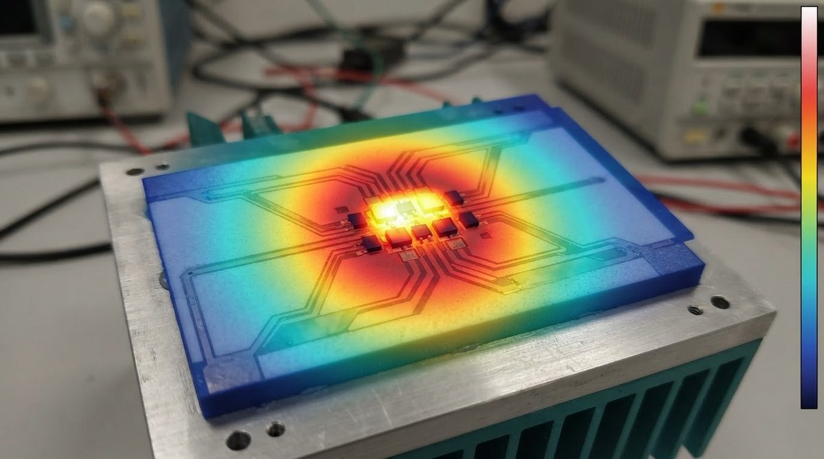
Alumina (Al₂O₃ 96%) is the workhorse ceramic substrate. It is less expensive, easier to machine, and available from every supplier. But its thermal conductivity tops out around 24–28 W/mK. When a bare die dissipates more than roughly 50 W/cm², the temperature drop across an alumina substrate becomes the bottleneck. AlN cuts that thermal resistance by a factor of 6–8, which can mean the difference between a passively cooled module and one that needs forced liquid cooling.
Copper is the metallization of choice because its bulk thermal conductivity (~400 W/mK) and electrical resistivity (1.7 µΩ·cm) outperform silver and gold in most power and thermal applications. If your design instead calls for copper-metallized alumina substrates, the same process families apply—but the thermal math changes significantly.
Four Ways to Bond Copper Metallized AlN Substrates
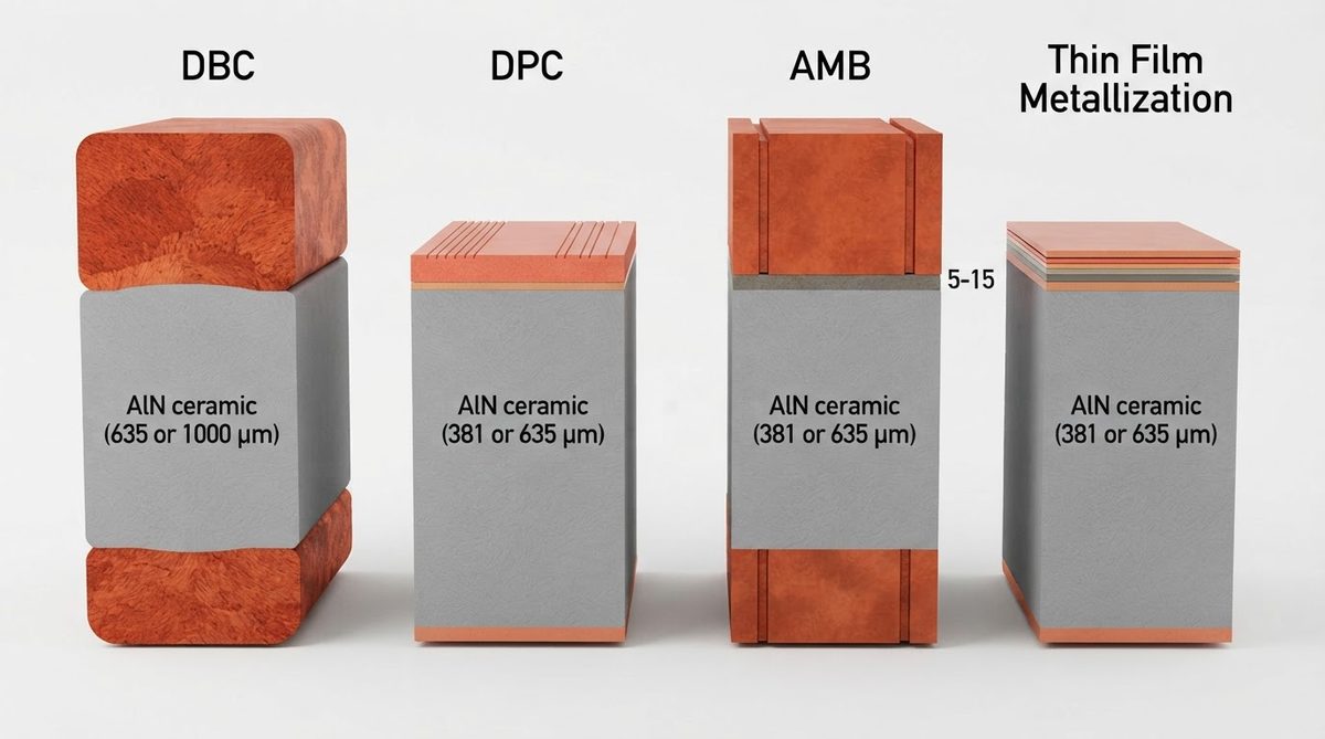
Each metallization process serves a different design window. The table below summarizes the trade-offs for copper metallized AlN across all four methods.
| Parameter | DBC | DPC | AMB | Thin Film |
|---|---|---|---|---|
| Cu thickness range | 0.15–0.50 mm | 1–200 µm | 0.15–0.80 mm | 1–20 µm |
| Min trace / space | ~200 µm / 200 µm | ~50 µm / 50 µm | ~250 µm / 250 µm | ~20 µm / 20 µm |
| Bond mechanism | Cu–O eutectic (~1065 °C) | Sputter seed + electroplate | Ag-Cu-Ti braze (~850 °C) | Sputter adhesion + seed |
| Thermal-cycle reliability (–40/+150 °C) | Good (500–1 000 cycles typical) | Good for thin Cu | Excellent (>3 000 cycles typical) | Limited by thin Cu |
| Typical applications | IGBT modules, power diodes | LED submounts, sensor circuits | SiC/GaN power modules, EV inverters | RF, MEMS, precision resistors |
Typical values for commercially available material, for comparison only. Confirm against the datasheet for your specific grade.
DBC (Direct Bonded Copper)
DBC heats a pre-rolled copper sheet in a controlled O₂ atmosphere until a thin Cu₂O layer forms at the interface, wetting and bonding to the AlN surface at ~1065 °C. The result is a mechanically strong, void-free joint with thermal resistance below 0.01 °C·cm²/W at the bond line. Standard copper thicknesses are 0.127 mm (5 mil), 0.254 mm (10 mil), and 0.30 mm (12 mil). For AlN DBC substrates, surface preparation of the AlN is critical because native aluminum oxide on the ceramic must be managed to achieve a reliable bond.
DPC (Direct Plated Copper)
DPC starts with a sputtered Ti or TiW adhesion layer (~50–200 nm), followed by a Cu seed layer (~200–500 nm), then pattern plating of copper to the target thickness. Because lithography defines the traces, DPC achieves much finer features than DBC. This makes it the preferred copper metallized AlN process for LED submounts, laser diode carriers, and compact sensor circuits. See more detail on AlN DPC substrates.
AMB (Active Metal Brazing)
AMB uses a braze alloy containing an active element—almost always titanium—that reacts with the AlN surface to form a TiN interface layer. Brazing occurs in vacuum at ~850 °C, well below the Cu–O eutectic temperature. The lower process temperature produces less residual stress, and the resulting bond survives more than 3 000 thermal cycles between –40 °C and +150 °C in published reliability data (per Rogers / curamik application notes). AMB is the standard for automotive-grade SiC and GaN power modules where JEDEC qualification demands extreme cycling endurance. Full process details are on the AlN AMB substrate page.
Thin Film
Thin-film metallization sputters the full copper stack (adhesion layer + conductor) and patterns it by photolithography and wet or dry etching. Copper stays below ~20 µm, so current-carrying capacity is limited. The payoff is line/space resolution under 30 µm, tight impedance control, and the ability to integrate thin-film resistors (TaN, NiCr) on the same substrate. RF power amplifier pallets and precision sensor bridges are the primary use cases. More on AlN thin-film substrates.
Worked Example: Thermal Resistance Comparison
Consider a 10 mm × 10 mm bare die dissipating 80 W. The substrate is 0.635 mm (25 mil) thick. We compare one-dimensional thermal resistance through the ceramic only (ignoring copper and solder layers):
Rth = t / (k × A)
- AlN (k = 180 W/mK): Rth = 0.000635 / (180 × 0.0001) = 0.035 °C/W → ΔT = 80 × 0.035 = 2.8 °C
- 96% Al₂O₃ (k = 26 W/mK): Rth = 0.000635 / (26 × 0.0001) = 0.244 °C/W → ΔT = 80 × 0.244 = 19.5 °C
That 17 °C difference at the substrate alone can shift junction temperature from within spec to dangerously close to derating. This is the core reason designers move from alumina to copper metallized AlN.
Enter your substrate area, thickness, and dissipated power below to estimate junction temperature rise for your own copper metallized AlN design.
Material Properties of AlN
| Property | Value | Unit | Condition | Source |
|---|---|---|---|---|
| Thermal conductivity | 170–200 | W/mK | 25 °C | Kyocera SH-30 / Maruwa AN-230 |
| CTE | 4.5–5.0 | ppm/°C | 25–400 °C | Kyocera SH-30 |
| Flexural strength | 300–400 | MPa | 3-point bend, ASTM C1161 | Maruwa AN-230 |
| Dielectric strength | 15–17 | kV/mm | 25 °C, 0.635 mm thick | CoorsTek ADS-996 |
| Dielectric constant (εr) | 8.5–9.0 | — | 1 MHz, 25 °C | Kyocera SH-30 |
| Volume resistivity | >1014 | Ω·cm | 25 °C | Maruwa AN-230 |
Typical values for commercially available material, for comparison only. Confirm against the datasheet for your specific grade.
When Not to Use Copper Metallized AlN
Cost sensitivity. AlN substrates cost 3–5× more per unit area than 96% alumina. If your thermal budget works on alumina, stay there.
Low-power or low-frequency circuits. Standard FR-4 or metal-core PCB handles most designs below ~10 W total dissipation with adequate heatsinking.
Extreme thermal cycling with thick copper. If your qualification requires >3 000 cycles at –55/+175 °C and you need >0.3 mm copper, silicon nitride (Si₃N₄) substrates with AMB offer higher fracture toughness (6–7 MPa·√m vs. 2.5–3.5 for AlN) and better survival rates.
Large panel sizes. AlN is typically available in substrates up to ~190 mm × 140 mm. Designs needing larger single-piece substrates may need to panel on alumina or use an IMS approach.
Frequently Asked Questions
Can you solder directly to copper metallized AlN?
Yes. Standard Sn-Ag-Cu (SAC305) and Au-Sn (80/20) solders wet well to copper metallized AlN surfaces, especially with ENIG or ENEPIG finish. Preheat ramps should stay below 3 °C/s to limit thermal shock to the ceramic.
Does AlN degrade in humid environments?
Unprotected AlN hydrolyzes slowly in the presence of moisture, forming aluminum hydroxide on the surface. Copper metallization itself acts as a barrier on bonded areas. Exposed AlN edges or vias can be protected with a passivation layer (e.g., SiO₂ or Si₃N₄ thin film) or by hermetic packaging.
What surface finishes work on copper metallized AlN?
ENIG, ENEPIG, immersion silver, and electrolytic Ni/Au are all used. The choice depends on soldering method and wire-bond requirements. Au wire bonding typically requires electrolytic Ni/Au with a minimum 0.5 µm Au layer.
How does AlN compare to BeO for thermal performance?
Beryllium oxide (BeO) offers thermal conductivity of 250–300 W/mK, higher than AlN. However, BeO dust is a confirmed human carcinogen and causes chronic beryllium disease. Handling, machining, and end-of-life disposal require strict controls per OSHA 29 CFR 1910.1024. Most new designs have moved to AlN to avoid these hazards.
What is the maximum operating temperature for copper metallized AlN?
The AlN ceramic itself is stable above 1 000 °C. The practical limit is set by the copper metallization and bonding interface. DBC bonds degrade above ~600 °C in oxidizing atmospheres; AMB braze joints are rated to ~500–600 °C depending on alloy. In most power-electronic applications, the operating ceiling is 300–400 °C, limited by solder and packaging materials rather than the substrate.
Next Step
If your thermal analysis points to copper metallized AlN, the next decision is which metallization process fits your trace geometry, copper thickness, and reliability requirements. Review the comparison above, then request a quote with your substrate dimensions, copper spec, and target quantity.