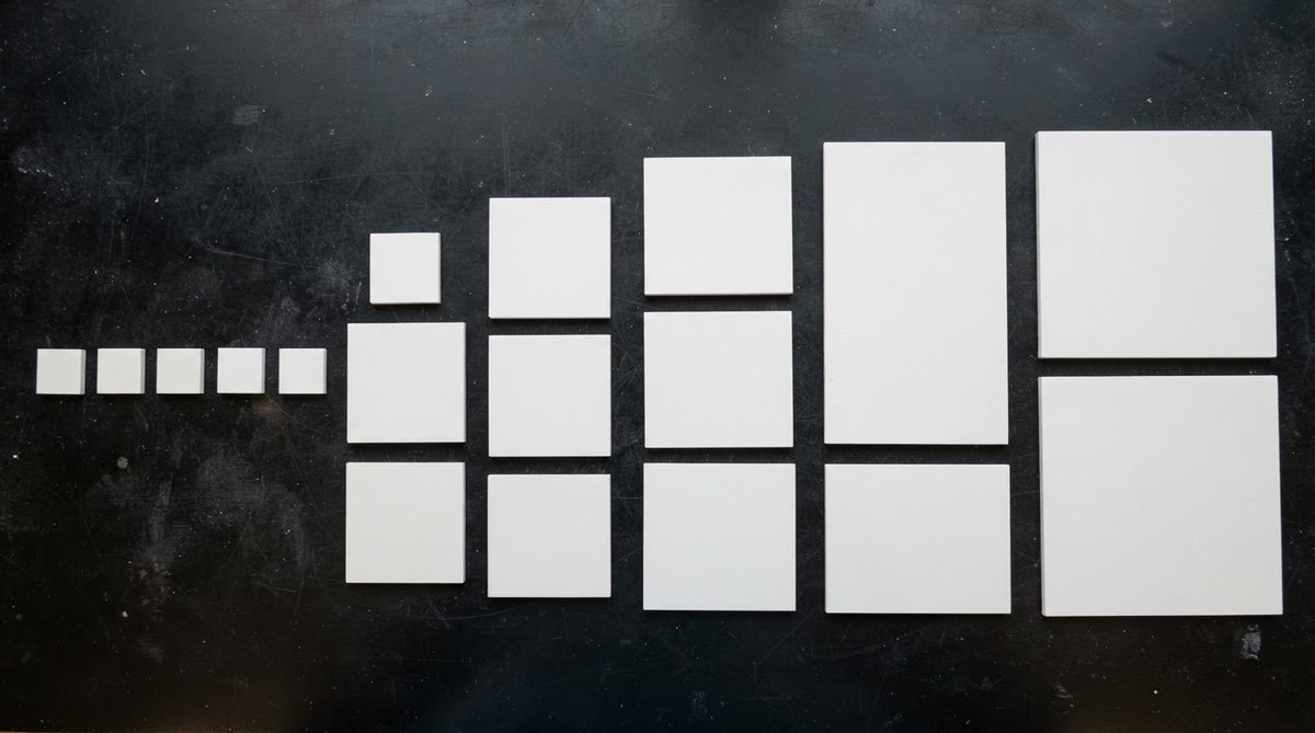
You can buy alumina substrates in two main purity grades—96% and 99.6% Al₂O₃—with stock sizes ranging from roughly 1″ × 1″ up to 4.5″ × 4.5″ or larger panels. The 96% grade covers most thick-film and general-purpose needs at lower cost. The 99.6% grade is reserved for thin-film circuits, high-frequency designs, and applications demanding tighter surface finish or higher thermal conductivity.
Key Takeaways
- 96% alumina substrates offer thermal conductivity of 24–28 W/mK at 25 °C and cost roughly 30–50% less per piece than 99.6% alumina.
- 99.6% alumina reaches 28–35 W/mK at 25 °C with a finer grain structure, enabling surface roughness below Ra 0.1 µm after polishing—critical for thin-film metallization.
- Standard stock sizes (2″ × 2″, 3″ × 3″, 4.5″ × 4.5″) ship faster than custom dimensions because the ceramic is already fired and inventoried.
- Every alumina substrate is brittle. Plan your handling, scribing, and packaging before ordering, not after breakage.
96% vs. 99.6% Alumina: Which Grade Do You Need?
The purity number refers to the Al₂O₃ content by weight. The remaining fraction is a glass-phase binder (typically SiO₂, CaO, MgO) that lowers sintering temperature and affects final properties. Higher purity means less glass phase, higher density, and better electrical and thermal performance—at higher cost.
For thick-film hybrid circuits, power resistor networks, and LED submounts, 96% alumina is the standard choice. Its surface roughness after as-fired processing (Ra 0.3–0.8 µm, per CoorsTek ADS-96R datasheet) is compatible with screen-printed conductors. If your circuit uses sputtered or evaporated thin-film metallization, the smoother surface of 99.6% alumina (Ra 0.025–0.1 µm after lapping) gives better adhesion and line definition.
| Parameter | 96% Al₂O₃ | 99.6% Al₂O₃ | Unit | Condition | Source |
|---|---|---|---|---|---|
| Thermal conductivity | 24–28 | 28–35 | W/mK | 25 °C | CoorsTek ADS-96R / ADS-996 |
| Dielectric constant (εr) | 9.0–9.5 | 9.7–10.0 | — | 1 MHz | Kyocera A-476 / A-493 |
| Flexural strength | 340–380 | 380–450 | MPa | ASTM C1161, 3-pt bend | CoorsTek datasheets |
| Surface roughness (as-fired) | 0.3–0.8 | 0.15–0.5 | µm Ra | — | Maruwa HA-96 / HA-996 |
| CTE | 7.2–8.0 | 7.1–7.9 | ppm/°C | 25–400 °C | CoorsTek datasheets |
| Typical cost index | 1.0× | 1.4–1.6× | relative | same size/thickness | Industry pricing |
Typical values for commercially available material, for comparison only. Confirm against the datasheet for your specific grade.
If your design needs a CTE match closer to silicon (2.6 ppm/°C) or GaN-on-SiC (4.3 ppm/°C), alumina may not be the right substrate—consider AlN or Si₃N₄ instead. For optical or UV-transparent applications, a quartz substrate or sapphire substrate is a better fit.
Standard Sizes and Thicknesses in Stock
Alumina substrates are typically stocked in a handful of standard ceramic substrate sizes. Buying a stock size avoids custom laser-cutting or diamond-scribing charges and cuts lead time from weeks to days. Common stock dimensions include:
- 1″ × 1″ (25.4 × 25.4 mm)
- 2″ × 2″ (50.8 × 50.8 mm)
- 2″ × 3″ (50.8 × 76.2 mm)
- 3″ × 3″ (76.2 × 76.2 mm)
- 4.5″ × 4.5″ (114.3 × 114.3 mm)
Standard thicknesses range from 0.25 mm (10 mil) to 1.0 mm (40 mil), with 0.381 mm (15 mil) and 0.635 mm (25 mil) being the most commonly inventoried. Thinner substrates reduce thermal resistance but are more fragile during handling and assembly. If your design requires a non-standard shape—slots, notches, rounded corners—expect a custom-shape machining step that adds cost and 5–10 business days to the schedule.
Choosing a Metallization Process
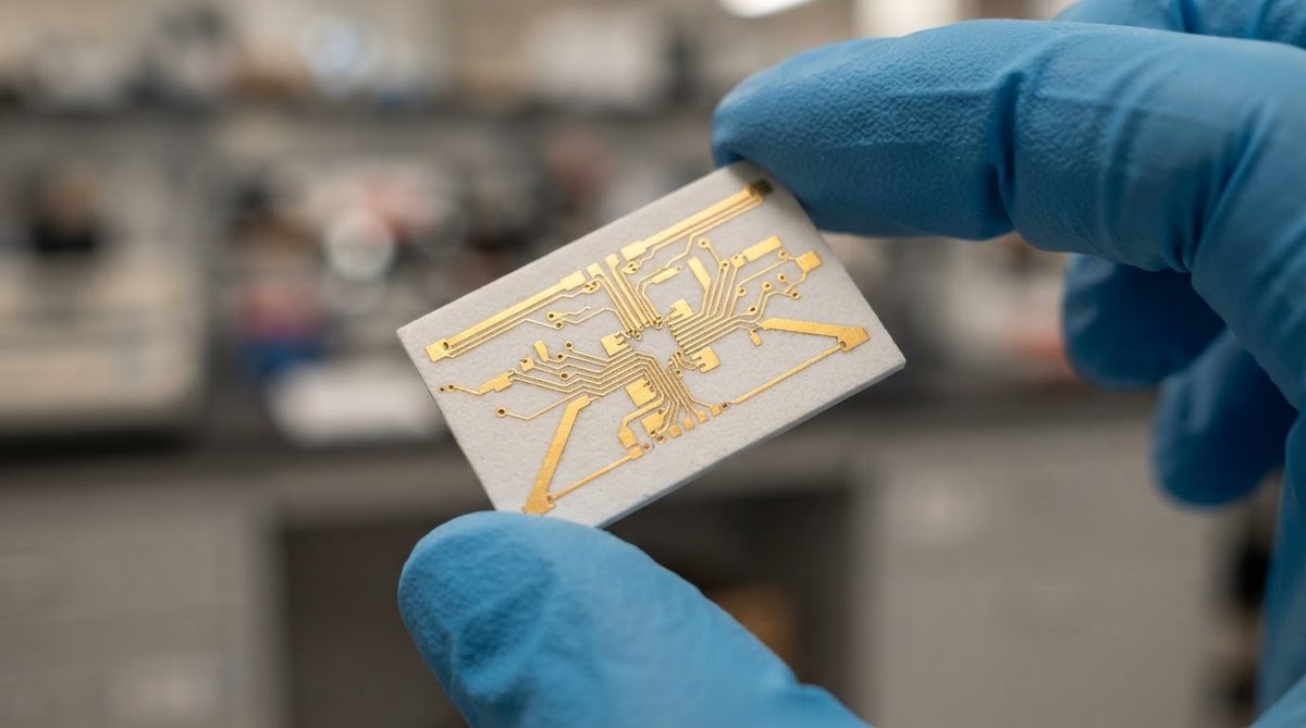
A bare alumina substrate is just the starting point. The metallization process determines your circuit’s trace resolution, copper thickness, and thermal performance. Here is a quick decision framework:
Thick film (screen print): Best for resistor networks, simple conductor patterns, and high-volume hybrid circuits. Line/space down to roughly 100–125 µm. Works well on 96% alumina. See the 96% thick-film substrate product page for details.
Thin film (sputter/etch): Required when you need line/space below 50 µm, tight resistor tolerance (±0.1%), or RF impedance control. Demands the smoother surface of 99.6% alumina. The 96% thin-film substrate page covers the lower-cost option where surface finish permits.
DBC (Direct Bonded Copper): For power modules needing 0.2–0.4 mm copper bonded directly to the ceramic. High current capacity, but limited to simple patterns. Alumina 96% DBC is the most cost-effective ceramic power substrate.
DPC (Direct Plated Copper): Combines sputtered seed layers with electroplating for fine features and moderate copper thickness (up to ~100 µm). Good balance of resolution and thermal spreading.
HTCC / LTCC: Co-fired multilayer structures. The ceramic and conductor are fired together, enabling buried vias and embedded passives. HTCC uses tungsten or moly-manganese conductors; LTCC uses silver or gold.
What to Specify When You Order
An incomplete purchase order is the most common cause of delays and rejects. Include all of the following in your RFQ:
- Grade: 96% or 99.6% Al₂O₃.
- Dimensions: Length × width × thickness, with tolerances (typical: ±0.1 mm on length/width, ±0.025 mm on thickness for ground substrates).
- Surface finish: As-fired, lapped, or polished. State the Ra target if critical.
- Edge condition: As-cut, chamfered, or ground. Sharp edges chip easily in automated pick-and-place.
- Metallization: Blank or metallized. If metallized, specify the process, conductor material, and pattern (Gerber file).
- Quantity and schedule: Prototype vs. production volumes affect unit price by 2–5×.
- Compliance: RoHS, REACH, or any restricted-substance requirements.
When Not to Buy Alumina
Alumina is the workhorse ceramic substrate, but it is not always the right one. Skip it when:
- Thermal conductivity above 35 W/mK is required. Aluminum nitride (AlN) provides 170–200 W/mK. The cost premium is justified for high-power-density GaN or SiC devices.
- Mechanical shock or vibration is extreme. Si₃N₄ offers roughly 2–3× the fracture toughness of alumina (6–8 MPa·m^0.5 vs. 3–4 MPa·m^0.5, per CeramTec data).
- Your board is large, low-power, and cost-sensitive. FR-4 or metal-core PCB will do the job for a fraction of the price.
- You need RF transparency or optical windows. Quartz and sapphire outperform alumina in those roles.
Frequently Asked Questions
What is the minimum order quantity for alumina substrates?
For stock sizes, MOQs can be as low as 5–25 pieces depending on the supplier and grade. Custom sizes or metallized substrates typically start at 25–50 pieces for prototypes, with pricing breaks at 100+ and 1,000+ units.
Can I get alumina substrates with holes or slots?
Yes. Holes and slots are cut by laser or diamond drilling either before or after firing. Minimum hole diameter is typically 0.1–0.2 mm depending on substrate thickness and the machining method. Specify hole positions and tolerances in your drawing.
How should I store alumina substrates before assembly?
Store substrates flat in cleanroom-grade wafer trays or interleaved with lint-free paper, in a dry environment (below 60% RH). Alumina is not moisture-sensitive like some organics, but surface contamination from handling oils or dust will degrade metallization adhesion.
Do alumina substrates need incoming inspection?
Yes, especially for thin-film work. Check dimensional tolerance with a micrometer, surface roughness with a profilometer (if Ra is spec’d), and visual defects under 10× magnification. Cracks from shipping are the most common reject cause—inspect edges carefully.
Is 96% alumina RoHS compliant?
Standard 96% and 99.6% alumina substrates are inherently RoHS compliant. The ceramic body contains no lead, mercury, cadmium, or other restricted substances. Metallization layers (especially thick-film pastes) may contain restricted materials, so confirm compliance for the complete assembly, not just the bare substrate.
Next Step
If you know your grade, size, and metallization process, request a quote with your specifications and Gerber files. For blank substrates, a dimensioned drawing is sufficient. Expect quoted pricing within one business day for standard configurations.