Thin film ceramic layout guidelines differ from thick-film and standard PCB rules because the metallization is sputtered or evaporated, then photo-lithographically patterned. That process delivers trace/space down to 10 µm on polished substrates, but it punishes design mistakes that would pass unnoticed on a thick-film board. The guidelines below cover geometry limits, substrate preparation, pad design, via integration, and the most common layout errors that kill yield.
What Makes Thin Film Layout Different
Thin film metallization starts with a blanket deposition of an adhesion layer (typically Ti or TiW, 20–100 nm) followed by a conductor layer (Au, Cu, or NiCr, 0.1–5 µm) applied by sputtering or e-beam evaporation. The pattern is defined by photoresist and wet or dry etching. Because the metal is deposited atom-by-atom onto a flat surface, feature resolution depends on three things: substrate surface finish, photolithography alignment, and etch uniformity.
Thick-film screen printing is limited to roughly 75–100 µm line/space by mesh and paste rheology. Thin film breaks through that floor by an order of magnitude, but the substrate must be polished to Ra ≤ 0.1 µm (per CoorsTek and Kyocera polished-grade datasheets) to avoid pin-holes and adhesion failures in the seed layer. If your design does not need features below 50 µm, thick-film layout rules may be more cost-effective.
Minimum Trace, Space, and Pad Geometry
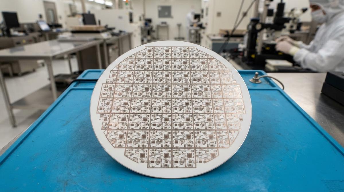
The table below summarises achievable geometry for thin film on common ceramic substrates. Values assume a polished surface (Ra ≤ 0.1 µm) and a single-layer metallization of 0.5–2 µm Cu or Au.
| Parameter | Typical Minimum | Aggressive (lab-proven) | Condition |
|---|---|---|---|
| Trace width | 20 µm | 10 µm | 0.5 µm Cu on 96% Al₂O₃, stepper lithography |
| Trace space | 20 µm | 10 µm | Same |
| Pad-to-trace clearance | 25 µm | 15 µm | Wire-bond pad, Au metallization |
| Wire-bond pad size | 80 × 80 µm | 60 × 60 µm | 25 µm Au ball bond |
| Flip-chip pad pitch | 150 µm | 100 µm | Solder bump, Cu UBM |
| Alignment accuracy (layer-to-layer) | ±5 µm | ±2 µm | Contact aligner vs. stepper |
Typical values for commercially available thin film ceramic processes, for comparison only. Confirm against the datasheet for your specific grade.
Keep trace widths uniform within a functional block where possible. Large width transitions create etch-rate differences that widen the narrow trace and undercut the wide one. If you must change width, taper over a length at least 3× the width difference.
Substrate Selection and Surface Preparation
Substrate choice affects adhesion, thermal performance, dielectric loss, and cost. The three substrates most commonly used for thin film are:
- 96% Al₂O₃ — Workhorse grade. Thermal conductivity 24–28 W/m·K at 25 °C (per Kyocera A-493 datasheet). Polishes well. Lowest cost. Suitable for most RF, sensor, and hybrid circuit applications. See 96% alumina thin film substrates for available sizes and finishes.
- 99.6% Al₂O₃ — Finer grain structure (1–2 µm vs. 5–10 µm for 96%). Achieves Ra ≤ 0.025 µm after lapping. Better for ≤15 µm features and microwave circuits above 20 GHz. Details on 99.6% alumina thin film substrates.
- AlN — Thermal conductivity 170–200 W/m·K at 25 °C (per Maruwa AN-170 datasheet). CTE of 4.5 ppm/°C closely matches Si (3.0 ppm/°C) and GaN (3.2 ppm/°C). Required for high-power die attach where junction-to-substrate thermal resistance must stay below 0.5 °C/W. See AlN thin film substrates.
Regardless of material, the substrate must be lapped and polished before deposition. An as-fired Al₂O₃ surface has Ra of 0.3–0.8 µm, which causes seed-layer discontinuities. Specify Ra ≤ 0.1 µm for 20 µm features and Ra ≤ 0.05 µm for anything below 15 µm.
Worked Example: Trace Width for a 50 Ω Microstrip
A common thin film application is a 50 Ω microstrip on 254 µm (10 mil) 96% Al₂O₃ (εr ≈ 9.6). Using the standard microstrip formula (per IPC-2141A):
Given: Z₀ = 50 Ω, h = 254 µm, εr = 9.6, t = 1 µm (Au conductor).
Result: The required trace width is approximately 240 µm. This is well within thin film capability. If you needed 50 Ω on a 127 µm substrate, the width drops to roughly 115 µm — still comfortable, but tighter clearances to ground vias become critical.
Verify with a 2.5-D field solver (Sonnet, ADS Momentum) because the thin film conductor thickness (≤ 2 µm) is much less than one skin depth at frequencies below 5 GHz, increasing resistive loss. At 10 GHz the skin depth in Au is about 0.8 µm, so a 1 µm film carries most of the current.
Via Integration on Thin Film Ceramic
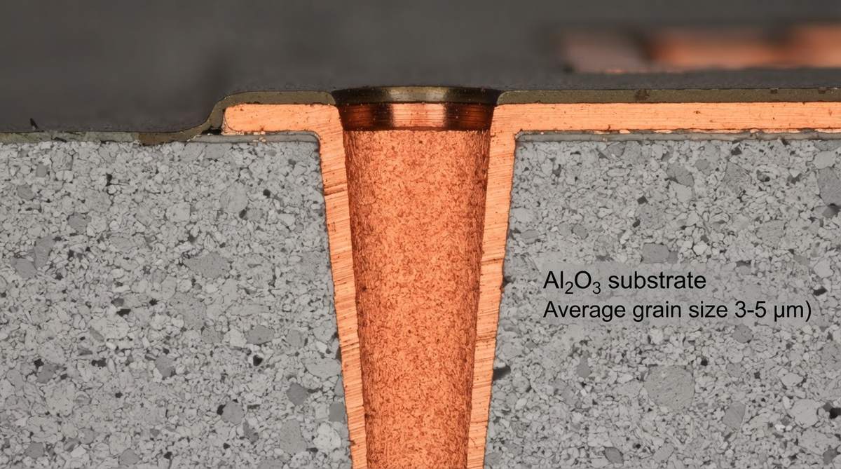
Thin film substrates are typically single-layer, but through-substrate vias are possible using laser drilling followed by fill metallization. Layout rules for vias on thin film ceramic:
- Minimum via diameter: 50–100 µm for laser-drilled vias in 254 µm Al₂O₃. Aspect ratio should stay below 3:1 to ensure reliable fill.
- Via-to-trace clearance: ≥ 50 µm from the via pad edge to the nearest unconnected trace. Sputtered metal can thin at the via rim, so the annular ring should be at least 30 µm wider than the via on each side.
- Via-to-edge clearance: ≥ 200 µm from any via centre to the substrate edge to avoid micro-cracking during laser scribing or panel break-out.
- Thermal vias: For die-attach pads, an array of vias on 300 µm pitch under the die reduces junction-to-backside thermal resistance by 30–50 % compared to a solid ceramic path. Confirm fill quality with X-ray inspection.
For detailed fill specifications, review via filling capabilities and tolerances.
Common Layout Mistakes That Reduce Yield
Acute-angle trace junctions. Angles below 90° create etch traps where resist lifts and metal remains, causing shorts. Use 45° or curved bends. Never use 90° bends in RF paths above 1 GHz.
Isolated metal islands smaller than 50 × 50 µm. Small features lose adhesion during lift-off or etch. If your design needs alignment marks or fiducials, size them at least 100 × 100 µm.
Mixing high-density and large-area copper on the same layer. Large ground planes etch more slowly than fine traces. The result is over-etched traces and under-etched planes. Split the ground plane into a hatched pattern with 50 µm lines and 50 µm gaps, or process the ground plane as a separate etch step.
Ignoring CTE mismatch at die attach. A bare-die GaAs device (CTE 5.7 ppm/°C) soldered to 96% Al₂O₃ (CTE 7.1 ppm/°C) sees moderate stress. But a large Si die (CTE 3.0 ppm/°C) on the same substrate needs a compliant attach or an AlN substrate to survive −55 °C to +125 °C thermal cycling per MIL-STD-883, Method 1010.
When Thin Film Ceramic Is Not the Right Choice
Thin film ceramic layout makes sense for fine features, tight impedance control, and low insertion loss. It is the wrong choice when:
- Your minimum feature is above 75 µm. Thick-film screen printing is faster, cheaper, and sufficient. The photolithography step adds cost with no benefit.
- You need thick copper (> 10 µm) for high current. Sputtered films are slow to build up. DBC or plated thick-film is better for power buses above 5 A.
- Budget is the primary constraint and volumes are low. Thin film tooling (masks, sputter targets, photoresist processing) has high NRE. For fewer than 50 units, evaluate whether a thick-film or DPC process meets your specs at lower cost.
- The board needs more than two routed layers. Thin film is inherently a single- or double-sided process. For complex routing, consider LTCC or a hybrid build.
Frequently Asked Questions
What is the thinnest trace achievable on a thin film ceramic substrate?
Production-proven minimum trace width is 10 µm on 99.6% Al₂O₃ polished to Ra ≤ 0.025 µm, using stepper lithography. Most production facilities quote 20 µm as a standard capability with contact aligners.
Can I use thin film metallization on an as-fired ceramic surface?
No. As-fired surfaces have Ra of 0.3–0.8 µm, which causes pin-holes and poor adhesion in sputtered seed layers. The substrate must be lapped and polished to Ra ≤ 0.1 µm before deposition.
How does thin film compare to DPC for fine-line ceramic circuits?
DPC (Direct Plated Copper) also uses photolithography on ceramic but builds thicker copper (5–50 µm) by electroplating. Thin film excels at sub-20 µm features and resistor integration (NiCr, TaN). DPC is better when you need higher current capacity with moderate line widths (25–75 µm).
Do I need a ground plane on the backside?
For microstrip RF circuits, yes. A continuous backside metallization serves as the ground reference. For DC sensor circuits or resistor networks, a backside ground is optional but improves thermal spreading if a heat sink is attached.
What adhesion layer should I specify?
Ti (20–50 nm) is the most common adhesion layer for Au and Cu conductors on Al₂O₃. TiW (50–100 nm) offers better barrier performance against Cu diffusion at elevated temperatures. Cr is an older choice being phased out due to RoHS concerns with hexavalent chromium in some etch chemistries.
Next Step
If your design needs thin film features on ceramic, prepare your Gerber files with the geometry rules above and request a design-for-manufacturability review. You can upload files and get a quote at AluminaPCB’s instant quote page.