Thick copper ceramic PCB capability spans copper layers from 70 µm (2 oz) up to 800 µm, depending on the metallization process. Direct Bond Copper (DBC) and Active Metal Brazing (AMB) are the two dominant methods for achieving heavy copper on alumina, aluminum nitride, or silicon nitride substrates. Electroplated copper build-up is also used for moderate thicknesses. Understanding thick copper ceramic PCB capability is essential for power-module and high-current designers because each method imposes different limits on trace width, spacing, adhesion strength, and thermal performance.
- DBC bonds pre-rolled copper foil (typically 127–300 µm) to Al₂O₃ or AlN at 1065–1083 °C using a Cu–O eutectic layer.
- AMB uses an active solder alloy (commonly AgCuTi) to braze copper foil (150–800 µm) onto Si₃N₄ or AlN at 780–900 °C.
- Plated copper can build thickness incrementally, reaching 50–150 µm with good adhesion when deposited over a sputtered or thick-film seed layer.
- Minimum trace/space widens as copper gets thicker: expect ≥ 200 µm trace/space at 300 µm copper, versus ≤ 100 µm at 70 µm copper.
- Thick copper on ceramic handles 50–120 A per cm of trace width (depending on thickness and cooling), far exceeding standard FR-4 heavy copper designs.
How Thick Can Copper Be on a Ceramic Substrate?
The answer depends on the bonding method. DBC is limited by the eutectic bonding mechanism, which works reliably with copper foils from about 100 µm to 300 µm on Al₂O₃ 96 % or AlN. Below 100 µm, DBC is possible but less common because thinner foils are harder to handle during the high-temperature bonding step. Above 300 µm, thermal stress during cooling can crack the ceramic.
AMB pushes the upper limit further. Because the braze alloy accommodates more CTE mismatch stress than a eutectic oxide bond, AMB can attach copper foils of 300–800 µm to Si₃N₄ substrates without cracking. Si₃N₄ is preferred for AMB at these thicknesses because its fracture toughness (6–7 MPa·m^0.5 per Kyocera SN-733 datasheet) is roughly 2× that of AlN and 3× that of Al₂O₃ 96 %. This range represents the upper end of thick copper ceramic PCB capability available today.
For designs that need moderate heavy copper (50–150 µm), electroplated copper on ceramic offers finer feature resolution than DBC or AMB because the copper is built up photolithographically rather than etched from a solid foil.
Thick Copper Ceramic PCB Capability: Trace and Space Tolerances
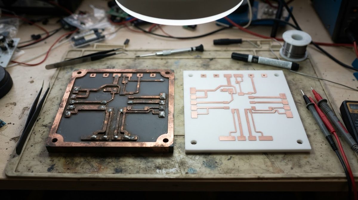
Etching thick copper foil on ceramic follows the same physics as on organic boards: the etch undercut grows roughly 1:1 with copper thickness. A 300 µm foil etched from one side will lose approximately 250–300 µm per edge, so the minimum practical trace width is about 1.5–2× the copper thickness. The table below summarizes typical capabilities.
| Copper thickness (µm) | Min trace width (µm) | Min space (µm) | Method | Typical tolerance (±µm) |
|---|---|---|---|---|
| 70 | 100 | 100 | DBC etch / plating | ±20 |
| 127 | 150 | 150 | DBC etch | ±30 |
| 200 | 250 | 200 | DBC etch | ±40 |
| 300 | 400 | 300 | DBC / AMB etch | ±50 |
| 500 | 600 | 500 | AMB etch | ±60 |
Typical values for commercially available DBC and AMB substrates. Confirm against the datasheet for your specific grade and supplier.
If your design requires finer features than DBC etching allows at a given thickness, consider a hybrid approach: a thinner DBC or plated base with selective copper plating to build up bus bars and thermal pads. Review the design rules for thick-film ceramic layouts to understand how seed-layer geometry constrains plated copper patterns.
Current-Carrying Capacity: A Worked Example
A common reason to push thick copper ceramic PCB capability to its limits is high continuous current. Here is a simplified estimate for a copper trace on an Al₂O₃ DBC substrate.
Given: 200 µm copper, 5 mm wide trace, 30 mm long, ambient 25 °C, substrate mounted on a heat sink with thermal grease (total Rth substrate-to-ambient ≈ 3 °C/W).
Step 1 — Trace resistance. Resistivity of copper at 80 °C ≈ 2.1 × 10⁻⁸ Ω·m. Cross-section = 0.2 mm × 5 mm = 1 × 10⁻⁶ m². R = ρL/A = (2.1 × 10⁻⁸ × 0.03) / 1 × 10⁻⁶ = 0.63 mΩ.
Step 2 — I²R loss at 60 A. P = 60² × 0.63 × 10⁻³ = 2.27 W.
Step 3 — Temperature rise. ΔT = P × Rth = 2.27 × 3 = 6.8 °C. Trace temperature ≈ 32 °C. Well within limits.
Enter your own trace dimensions, copper thickness, and current to estimate temperature rise for your specific layout.
On FR-4, the same 60 A would require a 5 mm wide, 200 µm copper trace too, but the board’s thermal resistance would be 5–10× higher, pushing trace temperature above 80 °C. The ceramic substrate’s thermal conductivity (24–28 W/mK for Al₂O₃ 96 %, per CoorsTek ADS-96R datasheet) spreads heat laterally and vertically far more effectively. This thermal advantage is a core part of thick copper ceramic PCB capability that organic substrates cannot match.
DBC vs. AMB vs. Plated Copper: Which Method to Specify
The choice depends on copper thickness, substrate material, and thermal-cycling reliability requirements. Each method defines a different envelope of thick copper ceramic PCB capability.
| Parameter | DBC | AMB | Plated build-up |
|---|---|---|---|
| Copper range | 100–300 µm | 150–800 µm | 5–150 µm |
| Substrate materials | Al₂O₃, AlN | Si₃N₄, AlN, Al₂O₃ | Al₂O₃, AlN, Si₃N₄ |
| Bond strength | ≥ 3 N/mm (peel, per IEC 60249-2) | ≥ 5 N/mm | ≥ 1.5 N/mm (depends on seed) |
| Thermal cycle life (−40/+150 °C) | 2,000–5,000 cycles (Al₂O₃) | 5,000–15,000+ cycles (Si₃N₄) | 1,000–3,000 cycles |
| Min trace/space at max Cu | 400/300 µm | 600/500 µm | 75/75 µm |
| Typical application | IGBT modules, LED COB | SiC/GaN power modules, EV inverters | RF, sensors, mixed-signal |
Values represent industry-typical ranges. Confirm against your substrate vendor’s qualification data.
For power modules that will see aggressive thermal cycling (automotive, traction), AMB on Si₃N₄ is the clear choice despite higher cost. For LED or industrial drives with moderate cycling, DBC on alumina is cost-effective. For designs where fine features matter more than raw copper thickness, thin-film copper deposition followed by plating gives the best resolution.
When Not to Use Thick Copper on Ceramic
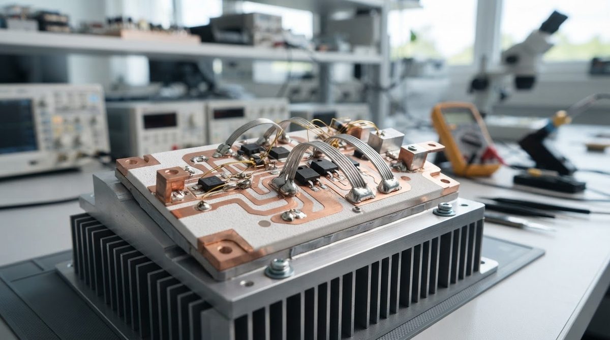
Thick copper ceramic substrates are expensive. A 150 × 100 mm DBC panel costs 5–15× more than an equivalent FR-4 heavy-copper board. If your design dissipates under 5 W total and operates below 130 °C, a metal-core PCB (MCPCB) or standard FR-4 with 2 oz copper and thermal vias will likely suffice at a fraction of the cost.
Thick copper also limits feature density. If your circuit requires 50 µm trace/space alongside high-current bus bars, a single thick-copper layer cannot do both. Consider a multilayer ceramic build that separates signal and power planes, or a hybrid approach with selectively plated regions.
Brittle ceramics and thick copper also create mechanical risk. Boards larger than about 50 × 50 mm with 300 µm copper can warp or crack if not designed with balanced metallization on both sides. Always specify copper on both faces, even if one side is an unbroken ground plane.
Frequently Asked Questions
Can I get 500 µm copper on alumina?
Not reliably with DBC. Alumina’s low fracture toughness (3–4 MPa·m^0.5) makes it prone to cracking under the thermal stress of bonding and cycling 500 µm copper. AMB on Si₃N₄ is the standard approach for copper above 300 µm.
Does thick copper affect the dielectric strength of the ceramic?
No. The ceramic’s bulk dielectric strength (≥ 10 kV/mm for Al₂O₃ 96 %) is unchanged by the copper. However, the copper edge profile after etching creates field concentrations. Wider trace spacing or edge passivation (glass overcoat) is recommended for designs above 2.5 kV isolation.
What surface finishes work on thick copper ceramic PCBs?
ENIG, ENEPIG, bare Ni/Au, and immersion silver are all compatible. The finish is applied after copper etching. For wire-bondable pads, electrolytic Ni/Au (3–5 µm Au) is standard. For soldering, ENIG (0.05–0.1 µm Au over 3–5 µm Ni) works well. Consult the thick-film metallization options page for finish details on printed conductors.
How do I specify balanced copper to prevent warpage?
Match copper thickness and coverage area on both sides of the substrate within 10–15 %. If the top side has 200 µm copper covering 60 % of the area, the bottom should have 200 µm copper covering at least 50–70 %. A full ground plane on the back side is the simplest solution.
Is thick copper ceramic PCB RoHS-compliant?
Yes. Copper, alumina, aluminum nitride, and silicon nitride contain no restricted substances under RoHS Directive 2011/65/EU. The solder alloy and surface finish determine overall RoHS status, not the substrate or copper layer.
Next Step
If you have a power module or high-current design that needs thick copper on ceramic, start by defining your copper thickness, minimum trace/space, and thermal-cycling requirements. These three parameters determine whether DBC, AMB, or plated copper is the right fit. Upload your design files for a thick copper ceramic PCB quotation to get specific tolerances and pricing for your layout.