Ceramic metallization is the process of bonding a conductive layer—typically copper, silver, gold, or tungsten—to a ceramic substrate so it can carry current, dissipate heat, or both. The method you choose fixes your minimum feature size, maximum current capacity, thermal resistance, and cost per board. Five processes dominate production: thick film, thin film, direct plated copper (DPC), direct bonded copper (DBC), and active metal brazing (AMB).
Key Takeaways
- Thick film prints conductors 100–250 µm wide using screen-printed pastes fired at 850–1000 °C; it is the lowest-cost route for simple patterns on Al₂O₃.
- Thin film sputters metal layers and achieves lines down to 10–20 µm, required for RF impedance matching and precision resistors.
- DPC combines sputtering with photolithography and electroplating, reaching 20–300 µm copper thickness with 30–50 µm line/space.
- DBC bonds a pre-formed copper sheet (typically 127–500 µm) to Al₂O₃ or AlN at the Cu–O eutectic (~1065 °C), handling currents above 100 A.
- AMB uses a Ti- or Zr-based braze alloy at 800–900 °C and is the preferred bond for Si₃N₄ substrates in EV traction modules.
Five Ceramic Metallization Methods Compared
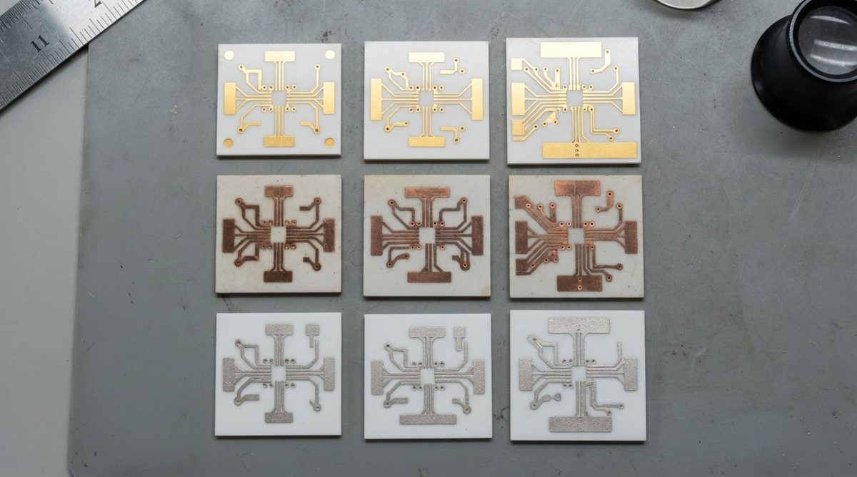
| Parameter | Thick Film | Thin Film | DPC | DBC | AMB |
|---|---|---|---|---|---|
| Conductor material | Ag, Au, Ag/Pd, W, Mo | Au, Cu, NiCr, TaN | Cu (sputtered + plated) | Cu sheet | Cu sheet + braze |
| Min line/space | 100–150 µm / 100 µm | 10–20 µm / 10–20 µm | 30–50 µm / 30–50 µm | ≥ 200 µm / ≥ 200 µm | ≥ 200 µm / ≥ 200 µm |
| Metal thickness | 5–25 µm (fired) | 0.1–5 µm | 20–300 µm | 127–500 µm | 127–800 µm |
| Firing / bonding temp | 850–1000 °C | Room temp (sputter); anneal ≤ 400 °C | Room temp (sputter + plate) | ~1065 °C (Cu–O eutectic) | 800–900 °C |
| Substrate compatibility | Al₂O₃, AlN, LTCC | Al₂O₃, AlN, quartz | Al₂O₃, AlN | Al₂O₃, AlN | Al₂O₃, AlN, Si₃N₄ |
| Typical application | Hybrid circuits, heaters, LEDs | RF, MEMS, precision resistors | High-density power, sensors | IGBT modules, power electronics | EV inverters, SiC modules |
| Relative cost (1 = lowest) | 1 | 3–4 | 2–3 | 2 | 3–5 |
Typical values for commercially available material, for comparison only. Confirm against the datasheet for your specific grade.
Thick Film Metallization
Thick film is the workhorse of ceramic metallization. A metal-glass paste—usually silver, gold, or silver-palladium—is screen printed onto the ceramic through a stainless-steel mesh, then dried and fired in a belt furnace at 850–1000 °C. The glass frit in the paste melts during firing and chemically bonds to the alumina surface, anchoring the conductor.
Fired thickness lands between 5 µm and 25 µm depending on mesh count and paste rheology. Sheet resistance for a silver conductor is typically 2–5 mΩ/□ at 12 µm fired thickness (per DuPont 6160 datasheet). That is adequate for LED thermal pads, heater traces, and low-frequency signal routing, but too resistive for high-current bus bars. For guidance on pattern layout, see the thick-film design rules reference.
Tungsten and molybdenum pastes are used in HTCC (high-temperature co-fired ceramic), where the metal is printed on green tape and co-fired at 1500–1600 °C. These refractory metals survive the sintering temperature of alumina but have higher resistivity (~5.5 µΩ·cm for W vs. 1.6 µΩ·cm for Ag). HTCC is common in hermetic military and aerospace packages.
Thin Film Metallization
Thin film deposits metal by sputtering or evaporation in a vacuum chamber, building layers from angstroms to a few microns. A typical stack on alumina is Ti/Pt/Au or TiW/NiCr/Au. The adhesion layer (Ti or TiW, 20–50 nm) bonds to the ceramic; the barrier layer prevents diffusion; the top layer carries current or accepts wire bonds.
Because patterns are defined by photolithography and wet or dry etching, thin film reaches 10–20 µm line/space—an order of magnitude finer than thick film. This precision makes it the only viable route for microstrip lines above 10 GHz, integrated thin-film resistors (TaN, NiCr with ±0.1% trimming), and MEMS sensor electrodes. Consult the thin-film layout guidelines for impedance-controlled trace geometry.
The trade-off is cost. Sputtering equipment is capital-intensive, throughput is lower than screen printing, and each additional metal layer adds a deposition-plus-etch cycle. For boards that do not need sub-50-µm features, thick film or DPC is almost always more economical.
DPC (Direct Plated Copper)
DPC combines vacuum deposition with electroplating. A thin seed layer of Ti/Cu (typically 50 nm Ti + 300 nm Cu) is sputtered onto the ceramic. Photoresist is applied and patterned, then copper is electroplated into the open areas to the target thickness—commonly 20–100 µm, though thick copper builds up to 300 µm are possible. After stripping resist and etching the seed, the result is a dense, void-free copper conductor directly on the substrate.
DPC achieves 30–50 µm line/space at 50 µm copper thickness. Adhesion strength exceeds 20 MPa on 96% alumina (per peel-test data in Heraeus technical literature). Because the copper is electroplated rather than bonded as a sheet, DPC avoids the high-temperature eutectic step of DBC, reducing thermal stress on fragile AlN substrates.
Worked Example: Thermal Resistance Through a DPC Copper Layer
Assume a 10 mm × 10 mm copper pad, 100 µm thick, on 0.635 mm Al₂O₃ 96% (k = 25 W/mK). Thermal resistance through the copper layer alone:
Rθ,Cu = t / (k × A) = 0.0001 m / (385 W/mK × 0.0001 m²) = 0.0026 °C/W
Through the alumina beneath it:
Rθ,Al₂O₃ = 0.000635 / (25 × 0.0001) = 0.254 °C/W
The ceramic dominates. This is why selecting the right substrate material matters far more than adding copper thickness beyond a certain point. For temperature limits of the substrate itself, see maximum temperature ratings for ceramic PCBs.
DBC and AMB: Sheet-Copper Bonding
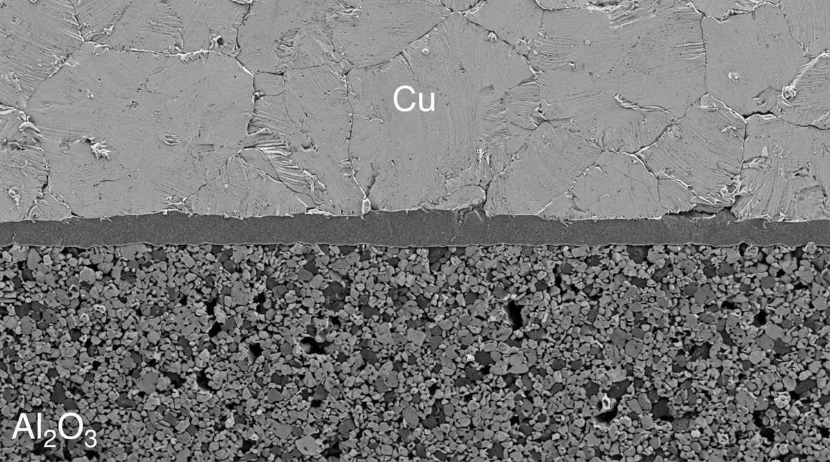
DBC (direct bonded copper) heats a copper sheet in a controlled-oxygen atmosphere to form a thin Cu₂O layer at ~1065 °C—just below copper’s melting point. That oxide wets the alumina or AlN surface and creates a direct ceramic-to-copper bond without adhesives. Copper thickness is typically 127 µm (5 mil), 254 µm, or 300 µm. DBC substrates from manufacturers such as Rogers curamik and Kyocera carry continuous currents above 100 A per trace in power module designs.
AMB (active metal brazing) replaces the oxide eutectic with a solder-like braze alloy containing an active element—usually titanium. The braze melts at 800–900 °C and reacts with the ceramic surface to form a TiN or TiO₂ reaction layer, then solidifies to anchor the copper. AMB is the only reliable method for bonding copper to Si₃N₄, whose high fracture toughness (6–7 MPa·√m per CoorsTek SN-90 datasheet) makes it the substrate of choice for automotive SiC traction inverters subjected to severe thermal cycling (-40 °C to +175 °C).
Both DBC and AMB produce coarse features (≥ 200 µm line/space after etching) and require chemical etching of the bonded copper sheet. They are not suitable for fine-pitch signal routing. In multilayer ceramic builds, DBC or AMB is often used only on the power layer, with thin-film or DPC handling the signal layers.
When NOT to Use Ceramic Metallization
If your board operates below 150 °C, carries less than 5 A, and needs more than four signal layers, standard FR-4 with plated copper vias will cost 5–20× less per unit area. Metal-core PCBs (MCPCB) handle up to 2–3 W/cm² thermal flux at a fraction of ceramic’s price. Choose ceramic metallization only when you need one or more of: operation above 300 °C, dielectric strength above 10 kV/mm, CTE matching to GaN or SiC die, or sub-50-µm features on an inorganic substrate.
Choosing the Right Method: A Decision Checklist
- Minimum feature size below 50 µm? → Thin film or DPC.
- Copper thickness above 127 µm? → DBC, AMB, or thick-copper DPC.
- Si₃N₄ substrate? → AMB only. DBC’s eutectic temperature can crack Si₃N₄ at the bond interface.
- Co-fired multilayer with internal conductors? → HTCC (W/Mo paste) or LTCC (Ag/Au paste) with co-firing during the sintering step.
- Budget-constrained, simple pattern? → Thick film screen print on 96% Al₂O₃.
Frequently Asked Questions
Can you plate copper directly onto bare alumina?
Not with electroless or electrolytic plating alone. Bare alumina has no catalytic surface for copper nucleation. You need a sputtered seed layer (Ti/Cu) first, which is the basis of the DPC process. Without it, adhesion will be near zero.
Does thick film silver migrate under DC bias?
Yes. Silver electromigration occurs at DC fields above roughly 2 V/mm in humid conditions (per IPC-9201 guidelines). For DC circuits with closely spaced conductors, use gold, copper (DPC), or a silver-palladium alloy with higher migration resistance.
What adhesion strength should I expect from DBC on AlN?
Peel strength for DBC on AlN is typically 8–15 N/cm, depending on the copper thickness and surface preparation. AMB on AlN generally exceeds 15 N/cm. Both values are well above the 4 N/cm minimum often cited in power-module qualification standards such as MIL-STD-883 Method 2019.
Is laser patterning an alternative to photolithography for ceramic metallization?
Laser ablation can pattern thick-film conductors after firing, achieving roughly 50–80 µm features. It is useful for prototyping and trimming resistors but slower than photolithography for volume production. It does not replace the deposition step—you still need a metallized surface to ablate.
How does metallization affect the CTE of the finished board?
A thick copper layer shifts the effective CTE of the assembly toward copper’s 17 ppm/°C. On a 0.635 mm Al₂O₃ substrate (CTE ~7 ppm/°C) with 0.3 mm copper on each side, the composite CTE rises to roughly 9–10 ppm/°C. This matters when you are die-attaching SiC (CTE ~4 ppm/°C); a thinner copper layer or an AlN substrate (CTE ~4.5 ppm/°C) reduces the mismatch.