Laser drilling ceramic substrates is the standard method for producing vias and through-holes in ceramic PCBs because mechanical drilling causes micro-cracking in brittle fired materials. CO₂ and UV solid-state lasers can form holes as small as 25–50 µm in alumina, aluminum nitride, and LTCC green tape, with positional accuracy within ±10–15 µm and minimal heat-affected zones when parameters are set correctly.
Key Takeaways
- UV lasers (Nd:YAG at 355 nm or excimer at 248 nm) produce the smallest vias (25–75 µm) with the least thermal damage when laser drilling ceramic substrates.
- CO₂ lasers (9.4–10.6 µm) drill faster and suit larger holes (≥100 µm), but leave wider heat-affected zones of 20–50 µm in alumina.
- LTCC green tape drills far more easily than fired substrates; vias are punched or laser-cut before ceramic firing and sintering, then shrink 12–16 % during co-firing.
- Aspect ratios above 5:1 in fired alumina require multiple-pass UV drilling and tight pulse-energy control to avoid taper and re-cast debris.
- Mechanical drilling is feasible only in green tape or very soft substrates; for fired Al₂O₃ and AlN, laser drilling ceramic is effectively the only production-viable option.
Why Mechanical Drilling Fails on Fired Ceramic
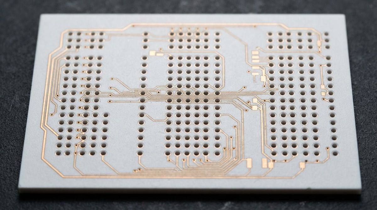
Fired 96 % alumina has a Vickers hardness of roughly 1400–1600 HV and a fracture toughness of only 3.5–4.0 MPa·√m (per CoorsTek ADS-996 datasheet). A carbide micro-drill bit generates point-contact stresses that exceed the ceramic’s fracture toughness, nucleating radial cracks from the hole edge. Even diamond-coated bits wear rapidly, and bit breakage inside the hole is common below 200 µm diameter.
Laser ablation avoids mechanical contact entirely. Material is removed by photon absorption—either thermal vaporisation (CO₂) or photo-chemical bond breaking (UV). The result is a clean hole wall with no propagating cracks, provided pulse energy stays within the process window. This is why laser drilling ceramic has become the default across the industry for via formation in fired substrates.
Laser Types Used for Laser Drilling Ceramic Vias
| Parameter | CO₂ (10.6 µm) | Nd:YAG UV (355 nm) | Excimer (248 nm KrF) |
|---|---|---|---|
| Min. hole diameter (fired Al₂O₃) | 80–100 µm | 25–50 µm | 25–40 µm |
| Typical drilling rate | 50–200 holes/s | 5–30 holes/s | 1–10 holes/s (mask projection) |
| Heat-affected zone | 20–50 µm | 5–15 µm | <5 µm |
| Taper (half-angle) | 3–7° | 1–3° | <1° (mask) |
| Capital cost | Low–medium | Medium–high | High |
| Best for | Through-holes ≥100 µm, high volume | Micro-vias, fine-pitch | Ultra-fine features, R&D |
Typical values for commercially available equipment. Confirm against your laser vendor’s process data for your specific substrate grade.
Most ceramic PCB production lines use a UV Nd:YAG or Nd:YVO₄ laser for fine features and a CO₂ laser for larger holes, selecting by diameter and throughput requirement. Excimer lasers appear mainly in research or very high-density packaging such as interposers for RF modules.
Material-Specific Behaviour During Laser Drilling Ceramic Substrates
96 % and 99.6 % Alumina (Al₂O₃)
Alumina absorbs well at both 10.6 µm and 355 nm. CO₂ drilling of 96 % alumina at 0.635 mm thickness typically requires 3–8 pulses per hole at 10–30 W average power, depending on hole diameter. The glassy grain-boundary phase in 96 % alumina melts preferentially, which can leave a thin re-cast layer (1–5 µm) on the hole wall. This layer is usually acceptable for ceramic metallization processes such as sputtering or plating, but should be characterised if the via carries high-frequency signals above 10 GHz.
99.6 % alumina has less glassy phase and ablates more cleanly, but requires slightly higher fluence per pulse because more energy goes into lattice disruption rather than melting the binder glass.
Aluminum Nitride (AlN)
AlN is transparent to CO₂ wavelengths below about 6 µm but absorbs at 10.6 µm. UV lasers at 355 nm also couple well. The main concern is oxidation: AlN exposed to air at temperatures above 700 °C forms Al₂O₃ on the hole wall, which degrades thermal conductivity locally. Drilling in a nitrogen or argon cover gas reduces this oxide layer. Expect 10–20 % slower drilling rates compared to alumina at the same thickness, due to AlN’s higher thermal conductivity (170–200 W/mK) wicking heat away from the ablation zone.
LTCC Green Tape
Green (unfired) LTCC tape is soft and drills easily. Holes are formed before lamination and firing, so the designer must account for the shrinkage factor—typically 12–16 % in X-Y and 15–20 % in Z, per the tape manufacturer’s datasheet (e.g., DuPont 951: 12.7 % ± 0.3 % X-Y). A via designed at 150 µm in the green state will finish near 130 µm after firing. Consult your LTCC co-fired ceramic design rules for minimum via-to-via pitch after shrinkage compensation.
Worked Example: Calculating Laser Passes for a 100 µm Via in 0.5 mm Alumina
Assume a 355 nm Nd:YAG laser with 50 µJ pulse energy, 20 kHz repetition rate, and a focused spot of 30 µm diameter.
- Fluence per pulse: Energy / spot area = 50 × 10⁻⁶ J / (π × (15 × 10⁻⁶)² m²) ≈ 70.7 J/cm². This exceeds the ablation threshold for alumina (~2–5 J/cm² at 355 nm per published data in Journal of the European Ceramic Society, Vol. 25, 2005), so material removal occurs each pulse.
- Removal rate: At this fluence, typical depth per pulse is 0.5–2 µm. Taking 1 µm/pulse as a midpoint, drilling through 500 µm requires ~500 pulses.
- Trepan path: For a 100 µm hole with a 30 µm spot, the beam must trepan a circle of ~70 µm diameter (100 µm minus one spot width). Circumference ≈ 220 µm. At 30 µm spot spacing, that is ~7 positions per revolution, so 500 / 7 ≈ 72 revolutions.
- Time per hole: 500 pulses at 20 kHz = 25 ms, plus galvo positioning overhead of ~5 ms. Total ≈ 30 ms per hole, or roughly 33 holes/s.
This estimate aligns with the 5–30 holes/s range in the table above. Actual rates vary with substrate grade, laser condition, and extraction system efficiency.
Enter your substrate material, thickness, hole count, and target diameter to estimate per-board laser drilling ceramic cycle time and relative cost impact.
Design Rules for Laser-Drilled Ceramic Vias
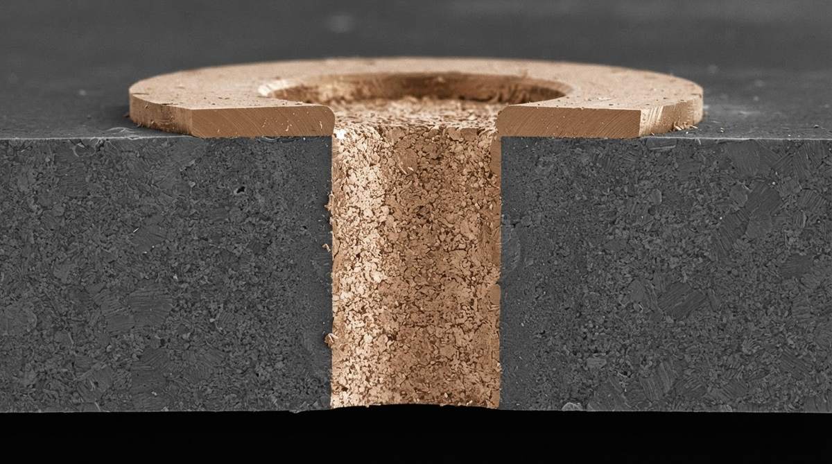
| Rule | Fired Al₂O₃ (UV laser) | AlN (UV laser) | LTCC green tape |
|---|---|---|---|
| Min. via diameter | 50 µm | 75 µm | 75 µm (pre-shrink) |
| Max. aspect ratio | 5:1 | 3:1 | 1:1 recommended |
| Min. via-to-via pitch | 2× via diameter | 2.5× via diameter | 2× via diameter (pre-shrink) |
| Min. via-to-edge clearance | 200 µm | 250 µm | 200 µm (pre-shrink) |
| Positional tolerance | ±10–15 µm | ±10–15 µm | ±25 µm (after shrink) |
Representative production values. Confirm against your fabricator’s capability sheet for the specific substrate and laser system in use.
Via pads for subsequent metallization should extend at least 50 µm beyond the hole edge on each side. For thin film ceramic design rules, sputtered seed layers require a clean, crack-free annular ring to ensure adhesion and electrical continuity through the via.
Laser Drilling vs. Laser Scribing
Both processes use similar equipment, but they serve different purposes. Laser drilling ceramic creates discrete holes for electrical vias or thermal paths. Laser scribing on ceramic cuts partial-depth grooves to define snap-apart panel outlines. Scribing uses a continuous or high-overlap pulse path at lower power, producing a V-groove typically 30–50 % of substrate thickness. The two operations are often performed on the same machine in sequence, but they require different parameter sets—confusing them risks cracking the substrate during scribing or under-drilling vias.
When Not to Use Laser Drilling
Laser drilling ceramic is unnecessary or suboptimal in several situations:
- FR-4 or metal-core PCBs: Standard mechanical CNC drilling handles these materials at far lower cost per hole. Laser drilling organic laminates is done only for micro-vias below ~100 µm.
- Very large holes (>1 mm) in ceramic: Ultrasonic machining or diamond grinding is faster and cheaper for holes above 1 mm diameter in fired substrates.
- Green-tape punching: For LTCC with via diameters above 150 µm and moderate density, mechanical punching is faster and less expensive than laser processing.
- Thick substrates (>2 mm): Laser drilling becomes impractically slow and taper becomes severe. Consider designing the via into the green body before sintering, or using a two-piece brazed assembly.
Frequently Asked Questions
Can you laser-drill a via in already-metallized ceramic?
Yes, but it is not recommended as standard practice. The laser must first ablate the metal layer, which has different absorption characteristics than the ceramic beneath. This can cause delamination of surrounding metallization within 50–100 µm of the hole. Drill first, then metallize.
Does laser drilling ceramic weaken the substrate?
Each hole is a stress concentrator, so flexural strength decreases as via density increases. For 96 % alumina, published data (ASTM C1161 four-point bend) shows a 10–20 % reduction in mean fracture strength at via densities above 25 vias/cm². Keep via-to-edge clearances above 200 µm to limit edge-initiated fracture.
What gas environment is needed during drilling?
Alumina can be drilled in ambient air. AlN should be drilled under nitrogen or argon cover gas to suppress surface oxidation. LTCC green tape is drilled in air with a vacuum extraction system to remove organic binder debris.
How do you inspect laser-drilled ceramic vias?
Optical microscopy checks diameter and position on the surface. For taper and sidewall quality, cross-sectioning with SEM imaging is the standard destructive method. X-ray inspection provides non-destructive verification of via fill quality after metallization, per IPC-6012 Class 3 requirements.
What is the cost impact of laser drilling ceramic on a board?
Laser drilling typically adds 5–15 % to the substrate processing cost, depending on hole count and diameter. A 25 mm × 25 mm alumina board with 200 vias at 100 µm might add 2–4 minutes of laser time. The cost driver is hole count, not hole size—smaller holes take more pulses but the galvo move time between holes dominates cycle time above a few hundred vias.