Edge plating castellation on ceramic PCBs creates metallized features along the board edge that allow direct side-soldering to a carrier or motherboard. Castellations are half-vias exposed by cutting through plated through-holes, producing a row of semicircular pads along one or more edges. Edge plating wraps a continuous copper strip around the board perimeter. Both techniques eliminate wire bonds or board-to-board connectors and reduce package height, which matters in high-density RF modules, sensor arrays, and power electronics.
Key Takeaways
- Edge plating castellation on ceramic substrates is formed by laser scribing or diamond-saw cutting through plated vias, then re-plating the exposed half-barrel.
- Typical castellation pitch on alumina (Al₂O₃ 96%) ranges from 0.5 mm to 1.27 mm; finer pitches require tighter substrate thickness and cutting tolerances.
- Edge plating thickness is usually 8–25 µm Cu plus a finish layer (ENIG, ENEPIG, or electrolytic Au), matching the surface finish on the rest of the board.
- Ceramic is harder to route than FR-4 (Mohs 9 for Al₂O₃ vs. ~3 for glass-epoxy), so tooling wear and micro-cracking at the castellation edge are the primary yield risks.
- LTCC substrates can form castellations during the green-tape stage before sintering, avoiding post-fire machining entirely.
What Is Edge Plating Castellation on a Ceramic PCB?
A castellation is a half-cylindrical metallized feature at the board edge, created when a plated through-hole is bisected during singulation. The resulting semicircle carries a solder-wettable surface that mates with a pad on the carrier board. During reflow, solder forms a fillet along the castellation wall, producing a mechanically and electrically sound joint visible for inspection. Edge plating, by contrast, wraps a continuous metal strip around the perimeter for grounding or EMI shielding. Together, edge plating castellation techniques give designers flexible options for side-mount interconnection on ceramic modules.
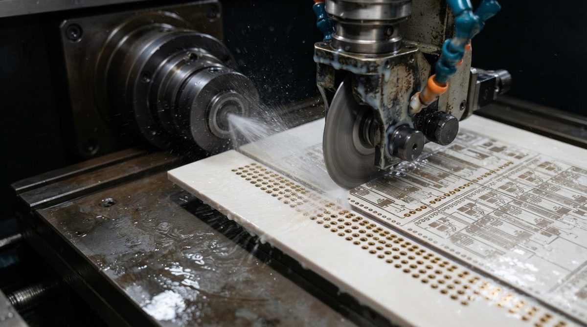
On organic PCBs, castellations are routine. On ceramics, the process is more demanding because the substrate is brittle and abrasive. Cutting must be precise enough to bisect each via cleanly without chipping the surrounding ceramic. Two common approaches exist: pre-fire shaping (for LTCC) and post-fire machining (for thick-film or thin-film on Al₂O₃ and AlN).
How Edge Plating Castellation Is Made on Ceramic Substrates
LTCC: Green-Tape Shaping Before Sintering
In LTCC co-fired ceramic design, vias are punched and filled with conductor paste while the tape is still soft. The panel outline, including castellation profiles, can be punched or laser-cut in the green state. After lamination and co-firing at 850–900 °C, the castellations are already formed. Post-fire touch-up may include a light abrasive step and a final plating pass to improve solder wettability.
Post-Fire Machining for Thick-Film and Thin-Film
For substrates metallized by thick-film or thin-film processes, the sequence is different. First, through-holes are laser-drilled or mechanically punched in the fired ceramic blank. Vias are then filled with conductor paste and the board goes through via filling and firing. After full metallization of both faces, the panel is singulated along a line that bisects each edge via.
Singulation uses diamond-blade dicing or laser scribing followed by mechanical break-out. Diamond dicing gives a cleaner edge but is slower. Laser scribing is faster for large panels but leaves a heat-affected zone that may need cleaning. After cutting, the exposed half-barrel is plated—typically electroless Ni/Au or electrolytic Cu followed by ENIG—to restore a uniform, solder-wettable surface. This final plating step is what distinguishes a finished edge plating castellation from a raw cut edge.
Edge Plating vs. Castellation: Which Do You Need?
Edge plating and castellation serve different purposes, though they share tooling. Edge plating wraps metal continuously around one or more board edges, providing a ground plane connection or EMI shielding path. Castellation provides discrete signal or power connections at defined pitches.
| Parameter | Edge Plating | Castellation |
|---|---|---|
| Geometry | Continuous strip along edge | Discrete half-vias at defined pitch |
| Primary function | Ground / shield wrap | Signal, power, or ground I/O |
| Typical Cu thickness | 10–25 µm | 8–20 µm on half-barrel wall |
| Min pitch | N/A (continuous) | 0.5 mm on Al₂O₃ 96%; 0.8 mm on AlN |
| Inspection | Visual + continuity | Visual fillet + X-ray if BGA-like |
| Main risk | Delamination at wrap corner | Chipping at half-via edge |
Typical values for commercially available material, for comparison only. Confirm against the datasheet for your specific grade.
Design Rules for Edge Plating Castellation on Ceramic
The rules below apply to Al₂O₃ 96% substrates with thick-film metallization. AlN and 99.6% alumina are machinable but require adjusted feed rates and tighter process control. For full thick-film ceramic design rules, see the dedicated page.
| Parameter | Recommended | Achievable (tighter tolerance) | Notes |
|---|---|---|---|
| Via diameter (before cut) | 0.3 mm | 0.2 mm | Finished castellation is half this diameter |
| Via-to-edge offset | 0 (centered on cut line) | ±25 µm alignment | Misalignment >50 µm causes asymmetric barrel |
| Castellation pitch | 1.0–1.27 mm | 0.5 mm | Below 0.5 mm, solder bridging risk rises sharply |
| Pad width on carrier board | 1.2× castellation diameter | 1.0× | Per IPC-7093 guidelines for castellated land patterns |
| Substrate thickness | 0.38–0.635 mm | 0.25 mm | Thinner substrates chip more easily during dicing |
| Edge chamfer | 0.05 mm × 45° | None | Chamfer reduces chipping but adds a process step |
Values based on typical Al₂O₃ 96% production. Confirm against your specific substrate and metallization supplier.
Worked Example: Castellation Count for a 10 × 10 mm Sensor Module
A 10 mm square ceramic module needs 24 I/O plus 4 ground castellations, distributed equally on all four edges—7 castellations per edge. At 1.0 mm pitch, the 7 castellations span 6.0 mm, leaving 2.0 mm of clearance per edge (1.0 mm at each corner). Via diameter before cut: 0.3 mm, giving a finished half-barrel radius of 0.15 mm. The carrier board pad should be at least 0.36 mm wide (1.2 × 0.3 mm). This is a comfortable edge plating castellation layout on 96% alumina with standard diamond-blade dicing.
If the same module shrank to 5 × 5 mm, fitting 7 castellations per edge would force 0.57 mm pitch—still above the 0.5 mm minimum but leaving almost no margin for dicing alignment error. At that point, consider reducing I/O count per edge or moving some connections to the bottom face as LGA pads.
Material Considerations for Castellated Ceramic Modules
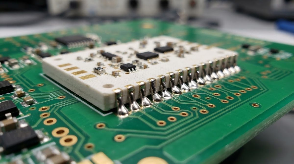
Al₂O₃ 96% is the most common substrate for edge plating castellation work. It machines predictably with diamond tooling and accepts thick-film metallization well. AlN (170–200 W/mK thermal conductivity per Maruwa datasheet, measured per ASTM E1461) is used when heat must exit through the castellation edge into a metal carrier, but AlN is more prone to micro-cracking during dicing. Si₃N₄ is extremely tough (fracture toughness 5–7 MPa·√m per CoorsTek data, ASTM C1421) but rarely castellated because its hardness makes post-fire machining slow and expensive.
For boards requiring heavy copper on ceramic, note that thick Cu layers (≥70 µm) at the castellation edge can cause burring during dicing. A two-step approach—dice first, then plate the edge—avoids this.
When Not to Use Castellations on Ceramic
Castellations are not always the right call. Skip them when:
- I/O count exceeds ~60 on a sub-10 mm module. At that density, a BGA or LGA pattern on the bottom face is more reliable and inspectable.
- The module will be wire-bonded anyway. Adding castellations to a board that already uses wire bonds for die attach adds cost without benefit.
- Thermal cycling is extreme (>1 000 cycles, –55 to +150 °C). The solder fillet on a castellation is small and sees concentrated strain. A brazed or sintered-silver die-attach joint on a DBC substrate handles this better.
- FR-4 or metal-core PCB meets the thermal and dielectric requirements. Castellations on organic boards cost a fraction of ceramic. Use ceramic only when you need the substrate properties—high thermal conductivity, low CTE, or high-frequency dielectric performance.
Inspection and Quality
Edge plating castellation quality is checked visually under 10–30× magnification. Acceptance criteria per IPC-7093 (Design and Assembly Process Implementation for Bottom Termination Components) include: no cracks extending from the half-barrel into the ceramic body, plating coverage ≥90% of the barrel wall, and no exposed base ceramic on the solder-wettable surface. After assembly, a good solder fillet should wet at least 75% of the castellation height. X-ray inspection is used when the fillet is not visible from the outside.
For metallization capabilities and tolerances specific to edge features, check the process spec before committing to a pitch below 0.8 mm.
Frequently Asked Questions
Can I reflow-solder a castellated ceramic module the same way as an organic one?
Yes. Standard SAC305 reflow profiles work. Peak temperature of 245–250 °C for lead-free solder is well within the operating range of any ceramic substrate. The main difference is CTE mismatch: ceramic (6–8 ppm/°C for Al₂O₃) vs. FR-4 carrier (14–17 ppm/°C). Use a compliant solder joint or match the carrier material to reduce stress.
What surface finish works best on castellations?
ENIG (3–5 µm Ni, 0.05–0.1 µm Au) is the most common finish for castellated ceramic modules. It provides good solder wettability and shelf life. Electrolytic Ni/Au (1–5 µm Au) is used for wire-bondable pads on the same board. Bare thick-film Au or Ag conductor is sometimes left unplated if the paste already provides a wettable surface.
How small can a castellation be on a ceramic PCB?
The smallest production castellation on Al₂O₃ 96% uses a 0.2 mm via, yielding a 0.1 mm radius half-barrel. Below this, via fill reliability drops and the half-barrel becomes too small for a reliable solder fillet. Most designs use 0.25–0.3 mm vias for margin.
Do castellations weaken the ceramic substrate mechanically?
They create stress concentrators at each half-via. Flexural strength of the singulated part drops roughly 10–20% compared to a plain edge, based on three-point bend tests (ASTM C1161) on castellated vs. non-castellated 96% alumina coupons. For substrates thinner than 0.25 mm, this can be significant. Adding a small chamfer at each castellation reduces the stress concentration.
Is edge plating possible on AlN ceramic?
Yes, but AlN requires a protective oxidation barrier (typically sputtered Ti/Pt or TiW) before Cu plating, because AlN hydrolyzes in alkaline plating baths. The added process steps increase cost by roughly 20–30% compared to the same feature on Al₂O₃.