Ceramic substrate cleaning is the single most influential pre-metallization step for adhesion quality. A 1 nm organic film or a few particles trapped between substrate and seed layer can cause blistering, peel-strength failures, or open circuits after thermal cycling. Every metallization method—sputtered seed layers for DPC, thick-film paste, or thin-film PVD—demands a surface free of hydrocarbons, particulates, and adsorbed water down to measurable thresholds.
Key Takeaways
- Contact-angle measurement below 10° (water droplet on cleaned surface) is a practical go/no-go criterion for adequate ceramic substrate cleaning before sputtering.
- Ultrasonic cleaning in DI water plus mild alkaline detergent removes most particulates, but plasma treatment is needed to strip the final monolayer of organics.
- AlN substrates require pH-controlled chemistries (pH 7–9) because strong acids and strong bases attack the surface and form aluminum hydroxide.
- Recontamination begins within minutes of cleaning; the interval between final clean and metallization should be under 30 minutes in a cleanroom environment.
Why Cleaning Matters More on Ceramic Than on FR-4
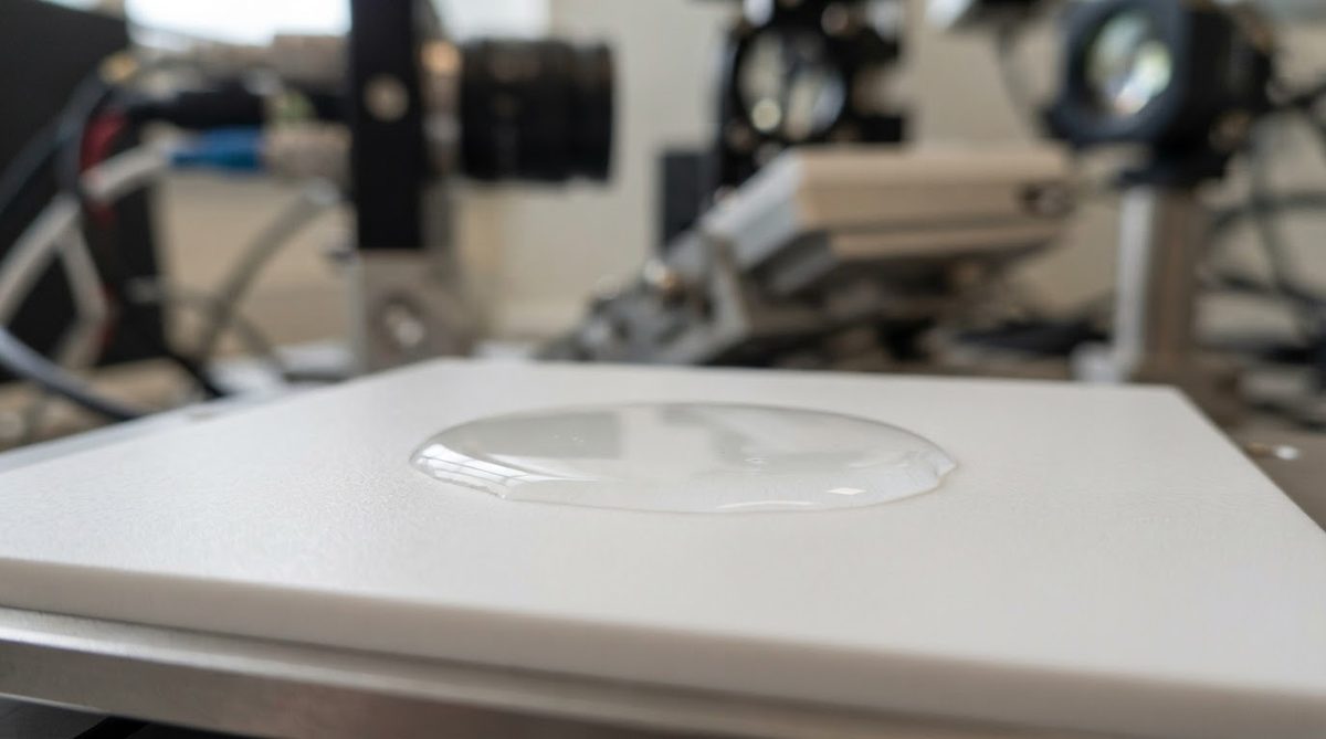
FR-4 surfaces are roughened copper foil, mechanically interlocked with prepreg. Ceramic substrates are dense, smooth, and chemically inert. Adhesion depends almost entirely on chemical bonding and van der Waals forces at the interface. Any contaminant layer—fingerprint oils, machining coolant, dust from lapping—inserts a weak boundary that fails under thermal stress.
Peel-strength data from Kyocera’s technical literature shows that a properly cleaned 96% Al₂O₃ substrate achieves >5 N/mm peel strength with sputtered Ti/Cu, while the same substrate with residual silicone contamination drops below 1 N/mm. That difference is entirely attributable to surface preparation.
Contaminant Types and Their Sources
| Contaminant | Typical source | Effect on metallization |
|---|---|---|
| Hydrocarbon films | Fingerprints, machining oil, tape residue | Reduces adhesion; causes blistering during soldering |
| Particulates (Al₂O₃ dust, fibers) | Lapping, scribing, handling | Creates voids under traces; short-circuits on fine-pitch patterns |
| Adsorbed water / hydroxyl groups | Ambient humidity | Outgasses during vacuum deposition; weakens Ti adhesion layer |
| Ionic residues (Na⁺, Cl⁻) | Tap water rinse, flux residue | Electrochemical migration, corrosion under bias |
| Silicone / PDMS | Mold release agents, certain tapes | Extremely difficult to remove; causes dewetting of paste and poor nucleation of sputtered films |
Sources: CoorsTek substrate handling guidelines; IPC-CH-65B (Guidelines for Cleaning of Printed Boards and Assemblies).
Standard Cleaning Sequence for Al₂O₃ Substrates
The following sequence is representative of what is used before ceramic metallization processes such as DPC and thin-film deposition. Adjust times and chemistries for your specific substrate grade.
- Gross degreasing. Immerse substrates in an alkaline detergent bath (pH 9–11, 50–60 °C) with ultrasonic agitation at 40 kHz for 5–10 minutes. This removes machining oils and handling residues.
- DI water cascade rinse. Three-stage overflow rinse in deionized water (≥18 MΩ·cm resistivity). Each stage 2 minutes minimum. Residual detergent left on the surface is as harmful as the original contaminant.
- Acid dip (optional). A brief dip in dilute HCl (1–5% v/v, room temperature, 1–2 minutes) removes metallic ion contamination. Skip this step for AlN—see the material-specific section below.
- Final DI rinse. Overflow rinse to resistivity ≥16 MΩ·cm in the drain.
- Drying. Spin dry or N₂ blow-off. Avoid compressed shop air, which contains oil mist. Oven bake at 120–150 °C for 15–30 minutes drives off adsorbed moisture.
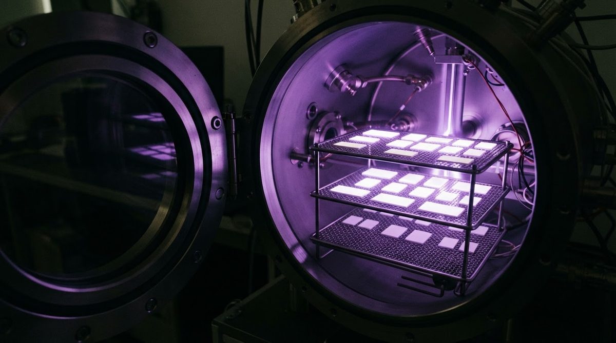
- Plasma cleaning. O₂ plasma at 100–300 W, 0.1–1.0 mbar, for 2–10 minutes. This ashes the last organic monolayer and activates the surface for bonding. Ar/O₂ mixtures (80/20) add mild physical sputtering for additional particulate removal.
After plasma cleaning, load substrates into the deposition chamber within 30 minutes. Every additional hour of exposure to ambient air adds roughly 0.3–0.5 nm of adsorbed hydrocarbon, per studies using XPS surface analysis (Watts & Wolstenholme, An Introduction to Surface Analysis by XPS and AES, Wiley, 2003).
Material-Specific Considerations
AlN (Aluminum Nitride)
AlN hydrolyzes in both strong acids and strong bases, forming Al(OH)₃ on the surface. Keep cleaning solutions in the pH 7–9 range. Replace HCl dips with a mild citric acid solution (2–3% w/v) if ionic cleaning is needed. Ultrasonic power should stay below 300 W to avoid micro-cracking on thin substrates (<0.38 mm).
Si₃N₄ (Silicon Nitride)
Si₃N₄ is chemically resistant to most cleaning agents. Standard alkaline/acid sequences work. The main risk is surface contamination from the lapping and polishing step that precedes metallization—diamond abrasive particles embed in grain boundaries. Extended ultrasonic cleaning (15 minutes at 40 kHz) or megasonic cleaning (0.8–1.0 MHz) is more effective at dislodging embedded particles than standard ultrasonic alone.
96% vs. 99.6% Al₂O₃
96% alumina contains a glassy silicate phase between grains. Aggressive alkaline cleaners (pH >12) can etch this grain-boundary glass, increasing surface roughness beyond specification. For substrates headed to thin-film patterning where Ra <0.1 µm matters, limit alkaline pH to 10 and shorten soak time.
Inspection and Acceptance Criteria
| Test | Method | Pass criterion | Reference |
|---|---|---|---|
| Contact angle (water) | Sessile drop, goniometer | <10° within 5 s | ASTM D7334 |
| Particulate count | Dark-field optical inspection or SEM | ≤5 particles >5 µm per cm² | Internal spec, aligned with ISO 14644-1 Class 5 |
| Surface carbon | XPS survey scan | <10 at% C on surface | — |
| Water break test | Visual: sheet flow, no beading | Continuous water film for ≥30 s | IPC-TM-650 2.3.38 |
Contact angle below 10° correlates strongly with peel strength above the 4 N/mm threshold for most sputtered metallizations on alumina.
Common Mistakes That Cause Adhesion Failures
- Skipping plasma cleaning. Wet cleaning alone leaves 1–3 nm of organic residue. For screen-printed thick-film pastes, this may be tolerable because the firing step burns off organics. For sputtered or evaporated thin films, it is not.
- Using shop-air blow-off. Oil-free N₂ or CDA (clean dry air) is mandatory. Shop air deposits a new hydrocarbon film instantly.
- Storing cleaned substrates overnight. Even in sealed containers, outgassing from packaging materials recontaminates surfaces. Clean and metallize on the same shift.
- Reusing rinse water. Cascade overflow rinse is not optional. Stagnant rinse tanks accumulate ionic and particulate contamination that redeposits on substrates.
When Cleaning Alone Is Not Enough
If substrate surface roughness is outside the window for your metallization process—too smooth for thick-film adhesion or too rough for fine-line thin-film—cleaning will not fix it. You need mechanical surface preparation first. Lapping to a controlled Ra (typically 0.2–0.6 µm for thick film, <0.1 µm for thin film) must precede the cleaning sequence. See lapping and polishing capabilities for achievable surface finishes.
Substrates with embedded grinding media, deep scratches, or edge chips should be rejected before cleaning. No amount of ultrasonic or plasma treatment removes a 20 µm diamond particle lodged in a grain boundary.
When Not to Use This Process
If your board is standard FR-4 or metal-core with pre-bonded copper foil, none of this applies—the copper is already mechanically adhered during lamination. Ceramic substrate cleaning protocols are specific to bare ceramic surfaces that will receive deposited or printed metallization. If you are using a DBC (direct bond copper) or AMB (active metal brazing) process where copper foil is bonded at high temperature in a controlled atmosphere, the cleaning requirements differ: the brazing filler metal wets the ceramic surface directly, and furnace atmosphere management matters more than pre-clean contact angle.
FAQ
Can I clean ceramic substrates in an ultrasonic bath with acetone?
Acetone is effective at dissolving many organics but evaporates rapidly, leaving residue streaks. It is also flammable and a poor choice for production environments. Alkaline aqueous detergent followed by DI water rinse gives more consistent results with lower safety risk.
How do I know if my substrate is clean enough?
The water-break test is the fastest in-line check: rinse the substrate with DI water and observe. If water sheets uniformly without beading for at least 30 seconds, the surface is acceptably free of organic contamination. For quantitative verification, measure contact angle with a goniometer—below 10° is the standard target.
Does plasma cleaning damage the ceramic surface?
O₂ plasma at typical parameters (100–300 W, under 10 minutes) does not measurably alter the surface roughness or mechanical strength of Al₂O₃, AlN, or Si₃N₄. Ar plasma at high power (>500 W) for extended durations can sputter-etch the surface, which may actually be desirable for adhesion promotion but must be controlled.
How long can I store substrates between cleaning and metallization?
Aim for less than 30 minutes in a cleanroom (ISO Class 5–7). In a standard production environment, recontamination is faster—15 minutes is a practical limit. If delays are unavoidable, store substrates in a N₂-purged desiccator and re-run plasma cleaning before metallization.
Is ceramic substrate cleaning different for thick-film vs. thin-film processes?
Yes. Thick-film pastes are fired at 850–1000 °C, which burns off residual organics during the firing cycle. The cleaning standard can be slightly relaxed. Thin-film sputtering or evaporation occurs at room temperature in vacuum, so every monolayer of contamination remains at the interface. Thin-film processes demand plasma cleaning and tighter contact-angle criteria.