AMB (active metal brazing) layout rules are driven by thick copper, high operating temperatures, and the CTE mismatch between copper and ceramic. Getting the geometry wrong causes substrate cracking, copper delamination, or thermal-cycling failure in fewer than 1,000 power cycles. This guide covers the dimensional rules, material pairings, and stress-management techniques that keep AMB substrates reliable in IGBT modules, SiC inverters, and other high-power assemblies.
What Is AMB and How Does It Differ from DBC?
Active metal brazing is a vacuum brazing process that bonds copper foil to a ceramic substrate using a braze alloy containing an active element—typically titanium. The titanium reacts with the ceramic surface to form a thin reaction layer (often TiN on AlN, or TiO on Al₂O₃), creating a chemical bond rather than the eutectic oxide bond used in DBC (direct bonded copper). This chemical bond is stronger and tolerates thicker copper.
DBC is limited to roughly 0.3 mm copper in production. AMB routinely handles 0.3–0.8 mm copper, and some suppliers offer up to 1.2 mm. The thicker copper carries higher current and spreads heat more effectively, but it also stores more elastic energy during thermal cycling, which means layout rules for AMB are stricter than for DBC.
Substrate Material Selection for AMB
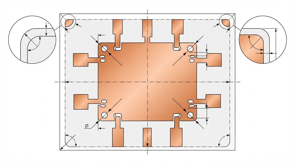
AMB works with Al₂O₃, AlN, and Si₃N₄. The choice affects every downstream layout decision.
| Parameter | Al₂O₃ 96% | AlN | Si₃N₄ | Unit | Condition |
|---|---|---|---|---|---|
| Thermal conductivity | 24–28 | 170–200 | 70–90 | W/mK | 20 °C |
| Flexural strength | 300–380 | 300–400 | 650–900 | MPa | ASTM C1161, 3-pt bend |
| Fracture toughness (K_IC) | 3.5–4.0 | 2.5–3.5 | 6.0–7.5 | MPa·m^½ | ASTM C1421 |
| CTE | 7.0–7.5 | 4.5–5.0 | 2.5–3.5 | ppm/K | 20–400 °C |
| Typical substrate thickness | 0.38–0.63 | 0.63–1.0 | 0.32–0.63 | mm | — |
Typical values for commercially available material, for comparison only. Confirm against the datasheet for your specific grade. Sources: Kyocera SN series datasheet; CoorsTek ADS-996 datasheet; Maruwa HA-series AlN datasheet.
Si₃N₄ dominates new EV traction inverter designs because its fracture toughness (6–7.5 MPa·m^½) is roughly double that of AlN, allowing it to survive more thermal power cycles with thicker copper. AlN remains the choice when raw thermal conductivity matters most—for example, in IGBT base plates where steady-state heat flux exceeds 100 W/cm². Al₂O₃ is cost-effective for lower-power industrial drives but cracks more readily under thick copper.
AMB Active Metal Brazing Layout Guidelines: Key Dimensions
The numbers below reflect production capabilities widely published by AMB substrate manufacturers (Kyocera, Rogers/curamik, Heraeus). Always confirm with your specific supplier’s design rules.
Copper Thickness
Standard AMB copper is 0.3 mm, 0.5 mm, or 0.8 mm. Thicker copper lowers electrical resistance and thermal spreading resistance but increases residual stress after brazing cool-down. On Si₃N₄ (0.32 mm), 0.8 mm copper on both sides is common. On AlN (0.63 mm), most designs stay at 0.3–0.5 mm to limit cracking risk.
Minimum Trace Width and Spacing
AMB copper is patterned by chemical etching after brazing. Because the copper is thick, the etch undercut is significant—roughly 1:1 for standard chemistry. Practical minimums:
- 0.3 mm copper: minimum trace width 0.4 mm, minimum gap 0.4 mm.
- 0.5 mm copper: minimum trace width 0.6 mm, minimum gap 0.6 mm.
- 0.8 mm copper: minimum trace width 1.0 mm, minimum gap 1.0 mm.
These are etched dimensions, measured at the ceramic surface. The top of the trace will be narrower than the bottom by approximately the copper thickness on each side (trapezoidal profile).
Edge Clearance (Copper to Substrate Edge)
This is the most critical AMB layout rule. Copper must not extend to the ceramic edge. The free ceramic border absorbs stress concentrations. A minimum clearance of 0.5 mm is typical for 0.3 mm copper; increase to 1.0 mm for 0.8 mm copper. Some designs use 1.5 mm for extreme thermal cycling requirements (–40 °C to +175 °C, >3,000 cycles).
Symmetry Between Top and Bottom Copper
AMB substrates warp if the copper area on top and bottom is unbalanced. The braze cools from roughly 850 °C to room temperature, and any asymmetry in copper coverage creates a bimetallic-strip effect. Best practice: match top and bottom copper area within 10%. If the circuit side has large etched gaps, add dummy copper pads on the back side to compensate.
Stress Management: Dimples, Slots, and Relief Patterns
Thermal cycling drives fatigue cracks in the ceramic, originating at copper pattern corners. Three layout techniques reduce peak stress:
- Corner rounding. All copper pad corners should have a radius ≥ 0.5 mm. Sharp 90° corners concentrate stress by 2–3× compared to a 1 mm radius, per finite-element studies published by Fraunhofer IISB.
- Stress-relief dimples. Small etched holes (0.5–1.0 mm diameter) near pad edges let the copper flex during thermal excursions. Place them 0.3–0.5 mm from the pad perimeter, spaced 2–3 mm apart.
- Isolation slots. For substrates larger than 40 × 40 mm, etch narrow slots (0.8–1.5 mm wide) between high-power and low-power zones. The slots interrupt crack propagation paths.
These techniques are especially important on AlN, which has lower fracture toughness than Si₃N₄. On Si₃N₄ substrates, dimples are sometimes omitted for simpler layouts, but corner rounding should never be skipped.
Worked Example: Copper-to-Edge Clearance Check
Suppose you are laying out a half-bridge SiC module on a 50 × 34 mm Si₃N₄ substrate (0.32 mm thick) with 0.8 mm copper on both sides. The high-side pad is 22 × 14 mm, and the low-side pad is 22 × 14 mm, placed side by side along the 50 mm axis.
Total copper width: 22 + 22 + gap = 44 + gap. With a 1.0 mm gap between pads and 1.0 mm edge clearance on each side: 1.0 + 22 + 1.0 + 22 + 1.0 = 47 mm. That fits within 50 mm with 1.5 mm to spare on each end—acceptable. If you had used only 0.5 mm edge clearance, the margin would be too tight for 0.8 mm copper at –40/+175 °C cycling. The extra 0.5 mm per side is worth the substrate area.
Surface Finish and Post-Braze Processing
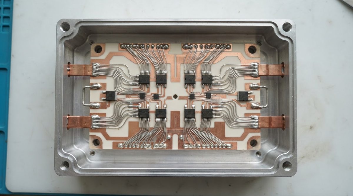
After etching, AMB substrates typically receive nickel plating (3–8 µm electroless Ni) followed by a thin gold or silver flash for solderability. The cleaning and surface preparation step before plating is critical: braze residue or oxide on the copper surface causes plating voids, which become solder voids under die attach.
For wire-bond pads, specify a minimum nickel thickness of 5 µm with gold ≥ 0.05 µm (per MIL-STD-883 for Au wire bonding). For solder die attach, silver finish (0.1–0.3 µm) over nickel gives better wetting than bare nickel.
When NOT to Use AMB
AMB is overkill—and over-budget—for many ceramic PCB applications. Choose a different process when:
- Copper ≤ 0.3 mm is sufficient. DBC is cheaper and widely available for 0.25–0.3 mm copper on Al₂O₃ or AlN.
- Fine traces are needed. If your design requires traces below 0.3 mm, consider DPC (direct plated copper) or thin-film metallization, which achieve 30–50 µm lines.
- Budget is constrained and power is moderate. Al₂O₃ thick-film substrates handle many LED and sensor applications at a fraction of AMB cost.
- Multilayer routing is required. AMB is a single-layer-per-side process. For embedded passives or multilayer interconnects, HTCC or LTCC is the right path.
FAQ
What is the maximum copper thickness for AMB?
Production AMB substrates are available with copper up to 1.2 mm, though 0.8 mm is the most common upper limit for standard product lines. Thicker copper requires wider trace spacing and larger edge clearances to manage residual stress.
Can I use AMB on alumina instead of Si₃N₄ or AlN?
Yes. AMB bonds well to 96% Al₂O₃. However, alumina’s lower fracture toughness (3.5–4.0 MPa·m^½) limits copper thickness to about 0.3–0.5 mm before thermal cycling reliability drops. For thick copper, Si₃N₄ is the preferred ceramic.
How many thermal cycles can an AMB substrate survive?
Si₃N₄ AMB substrates with 0.3 mm copper routinely pass >10,000 cycles at –40 °C to +150 °C (per IEC 60749-34 or similar profiles). With 0.8 mm copper on Si₃N₄, expect 3,000–5,000 cycles at the same range. AlN substrates typically achieve fewer cycles at equivalent copper thickness due to lower fracture toughness.
Do I need to match copper on both sides of the substrate?
Yes. Unbalanced copper causes substrate warpage during cool-down from the ~850 °C brazing temperature. Match top and bottom copper area within 10%, using dummy pads on the back if needed.
What braze alloy is used in AMB?
The standard alloy is Ag-Cu-Ti (silver-copper-titanium), typically around 72Ag-28Cu with 1–5% Ti by weight. The brazing temperature is 800–900 °C in vacuum (≤10⁻⁴ mbar). Titanium is the “active” element that wets the ceramic surface.
Is AMB compatible with lead-free solder die attach?
Yes. The nickel-plated, gold- or silver-finished surface of an AMB substrate is compatible with SAC305 and other lead-free solders. Ensure the nickel barrier is at least 3 µm to prevent copper dissolution into the solder during reflow.
Next Step
If you are designing a power module on AMB, prepare your layout with the clearance and symmetry rules above, then request a design-for-manufacturing review. Upload your Gerber files or DXF drawing for a DBC and AMB capabilities check or get a quote through the AluminaPCB homepage.