Aluminum nitride (AlN) substrates are commercially available in standard thicknesses from 0.25 mm to 2.0 mm, with 0.635 mm (25 mil) being the most widely stocked gauge. Understanding the full range of aluminum nitride AlN thickness options is essential because choosing the right gauge is a direct trade-off between thermal resistance, mechanical robustness, dielectric withstand voltage, and cost. Thinner substrates conduct heat better but break more easily; thicker ones survive handling but add thermal impedance.
Key Takeaways
- Standard aluminum nitride AlN thickness options are 0.25, 0.38, 0.50, 0.635, 1.0, and 2.0 mm; 0.635 mm is the default for most power-module designs.
- Typical thickness tolerance for as-fired AlN is ±0.05 mm; lapped and polished substrates can reach ±0.01 mm per Maruwa and Kyocera datasheets.
- Halving the substrate thickness roughly halves thermal resistance through the ceramic layer, all else equal.
- AlN thermal conductivity ranges from 170–200 W/mK at 25 °C depending on grain size and oxygen content (per CoorsTek and Kyocera published data).
- Dielectric breakdown voltage scales with thickness: a 0.635 mm AlN substrate withstands approximately 15–17 kV DC (per Maruwa datasheet, ASTM D149).
Standard Aluminum Nitride AlN Thickness Options
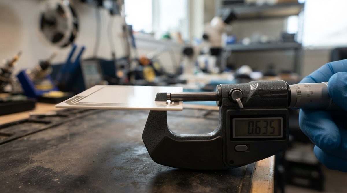
Most substrate manufacturers offer AlN in a set of standard gauges. Custom thicknesses are possible through grinding or lapping but add lead time and cost. The table below lists commonly available aluminum nitride AlN thickness options and their typical use cases.
| Thickness (mm) | Thickness (mil) | Typical Use Case | Availability |
|---|---|---|---|
| 0.25 | 10 | High-density power modules, LED submounts | Standard from major suppliers |
| 0.38 | 15 | DBC/AMB substrates for IGBT modules | Standard |
| 0.50 | 20 | RF packages, laser diode carriers | Standard |
| 0.635 | 25 | General-purpose power electronics, thick-film circuits | Most widely stocked |
| 1.0 | 40 | High-voltage isolation, structural substrates | Standard |
| 2.0 | 79 | Heatsink-integrated packages, mechanical carriers | Available on request |
Typical values for commercially available material, for comparison only. Confirm against the datasheet for your specific grade.
For designs that need substrates thinner than 0.25 mm, dedicated thin AlN ceramic substrates down to 0.15 mm are produced, though handling fragility and yield loss increase significantly below 0.25 mm.
Thickness Tolerances: As-Fired vs. Lapped vs. Polished
AlN substrates are manufactured by tape-casting and sintering. The as-fired surface has a roughness (Ra) of roughly 0.3–0.8 µm and a thickness tolerance of ±0.05 mm. For applications requiring tighter control, substrates are lapped or polished after firing. The finish you select interacts directly with which aluminum nitride AlN thickness options are practical for your metallization process.
| Finish | Thickness Tolerance | Surface Roughness (Ra) | Source |
|---|---|---|---|
| As-fired | ±0.05 mm | 0.3–0.8 µm | Kyocera SH-AlN datasheet |
| Lapped | ±0.025 mm | 0.1–0.4 µm | Maruwa HA-series datasheet |
| Polished | ±0.01 mm | <0.05 µm | CoorsTek ADS-996N datasheet |
Typical values for commercially available material, for comparison only. Confirm against the datasheet for your specific grade.
Polished substrates cost two to four times more than as-fired equivalents because of the extra machining steps. Specify polished only when your metallization process (thin-film sputtering, for example) demands it. Thick-film printing works fine on lapped or even as-fired surfaces.
How AlN Thickness Options Affect Thermal Resistance
The thermal resistance through the substrate is the simplest and most impactful parameter thickness controls. The one-dimensional conduction formula applies directly:
Rth = t / (k × A)
Where t is thickness (m), k is thermal conductivity (W/mK), and A is the heat-transfer area (m²).
Worked Example
Compare a 0.635 mm AlN substrate to a 0.38 mm substrate, both with k = 180 W/mK and a 10 mm × 10 mm die footprint (A = 1 × 10⁻⁴ m²):
- 0.635 mm: Rth = 0.000635 / (180 × 0.0001) = 0.035 °C/W
- 0.38 mm: Rth = 0.000380 / (180 × 0.0001) = 0.021 °C/W
Switching from 0.635 mm to 0.38 mm cuts the substrate’s thermal resistance by 40%. On a 200 W power module, that saves roughly 2.8 °C at the junction. Whether that matters depends on your overall thermal stack; if the solder layer and heatsink interface already dominate, thinning the AlN yields diminishing returns.
Enter your substrate area, thickness, and dissipated power below to estimate junction temperature rise for any of the aluminum nitride AlN thickness options you are considering.
For a broader comparison of how AlN stacks up against alumina and other ceramics, see the overview of ceramic substrate types compared.
Thickness and Dielectric Withstand Voltage
AlN has a dielectric strength of approximately 15–17 kV/mm (per Maruwa datasheet, tested to ASTM D149 at 25 °C). Dielectric withstand voltage scales roughly linearly with thickness for thin substrates:
- 0.25 mm → ~3.8–4.3 kV
- 0.38 mm → ~5.7–6.5 kV
- 0.635 mm → ~9.5–10.8 kV
- 1.0 mm → ~15–17 kV
If your design must meet a specific isolation rating (e.g., 5.7 kVrms per IEC 60664-1 for 1200 V SiC modules), thickness is non-negotiable. You cannot thin the substrate past the point where the required creepage and clearance are maintained. For more on the electrical properties that drive these decisions, see dielectric properties of ceramic substrates.
Mechanical Strength Considerations
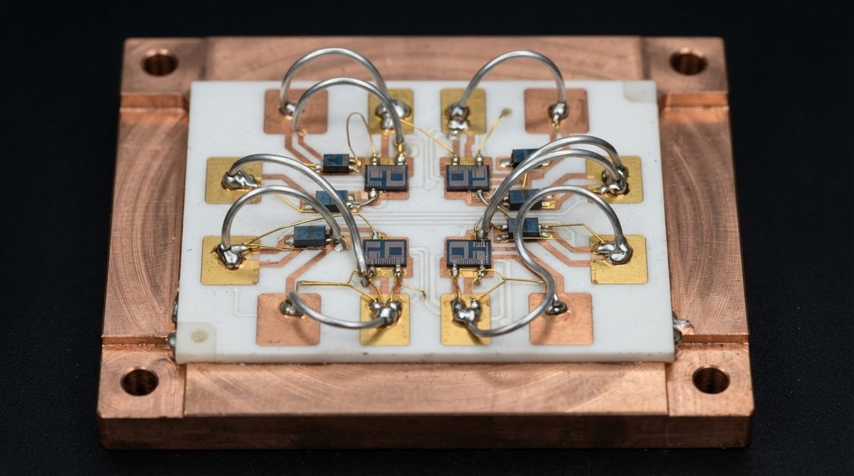
AlN is brittle. Its flexural strength is 300–400 MPa (three-point bend, ASTM C1161), lower than silicon nitride (Si₃N₄) at 600–900 MPa. Thinner substrates are more prone to cracking during handling, soldering, and thermal cycling. Below 0.38 mm, automated pick-and-place with vacuum tooling is strongly recommended over manual handling. Below 0.25 mm, yield losses during assembly can reach 5–10% unless the process is well controlled.
If mechanical robustness is the primary concern and your thermal budget allows it, silicon nitride’s material properties make it a better choice for thin substrates in high-vibration or high-cycle environments.
CTE and Thickness Interaction
AlN’s coefficient of thermal expansion is 4.5–5.0 ppm/°C (20–400 °C, per Kyocera datasheet). This is a close match to silicon (2.6 ppm/°C) and SiC (4.0 ppm/°C). A thicker substrate stores more strain energy during thermal cycling, which can increase the stress on solder joints at the die-attach interface. For large die (>10 mm × 10 mm) on thick substrates (>1.0 mm), finite-element analysis of the solder joint fatigue life is advisable. More detail on managing expansion mismatch is covered in the guide to CTE matching in ceramic PCB design.
When Not to Use AlN — or When to Pick a Different Thickness
AlN substrates are expensive: roughly 3–5× the cost per unit area of 96% alumina. If your thermal load is under 5 W/cm² and your operating temperature stays below 150 °C, a 96% Al₂O₃ substrate at 0.635 mm will likely suffice at a fraction of the price.
If you need extreme mechanical toughness in a thin gauge (≤0.32 mm), silicon nitride outperforms AlN in fracture toughness (6–7 MPa·√m vs. 2.5–3.5 MPa·√m). If your design is cost-sensitive and moderate thermal performance is acceptable, an aluminum-core MCPCB is a simpler, cheaper option. AlN earns its price only when the combination of high thermal conductivity, high electrical isolation, and CTE matching to semiconductor die is genuinely required. Reviewing all available aluminum nitride AlN thickness options against your thermal and mechanical budgets early in the design phase prevents costly respins later.
Frequently Asked Questions
What is the thinnest AlN substrate I can buy?
The thinnest standard AlN substrates are 0.25 mm (10 mil). Some suppliers offer 0.15 mm on a custom basis, but handling fragility and yield loss increase substantially. Below 0.25 mm, expect to qualify your assembly process carefully.
Does lapping change the thermal conductivity of AlN?
No. Lapping and polishing remove surface material but do not alter the bulk thermal conductivity of the ceramic. They do improve surface flatness, which can reduce thermal interface resistance at solder or bond layers by eliminating air gaps.
Can I get a non-standard AlN thickness like 0.75 mm?
Yes. Non-standard thicknesses are produced by grinding a thicker blank down to the target dimension. Lead times are typically 2–4 weeks longer than standard gauges, and minimum order quantities may apply.
How does AlN substrate thickness affect RF performance?
Thinner substrates reduce the distance between the signal trace and the ground plane, lowering the characteristic impedance for a given trace width. At microwave frequencies (>10 GHz), AlN’s low dielectric constant (8.5–9.0 at 1 MHz, per Kyocera) and low loss tangent (0.001–0.003) make it suitable, but impedance must be recalculated whenever thickness changes.
Is 0.635 mm AlN strong enough for wire bonding?
Yes. A 0.635 mm AlN substrate provides adequate support for both gold and aluminum wedge bonding. The substrate should be firmly clamped or soldered to a carrier during bonding to prevent flexure. Cracking during wire bonding is almost always a fixturing issue, not a substrate thickness issue.