A ceramic PCB prototype typically ships in 5–15 business days for standard alumina substrates with DPC or thick-film metallization, compared to 2–5 days for an FR-4 quick-turn. The longer cycle reflects tighter process controls, higher firing temperatures, and smaller supplier pools. Understanding what drives that timeline lets you plan around it instead of being surprised by it.
Key Takeaways
- 96% Al₂O₃ prototypes are the fastest and cheapest ceramic option, often 5–10 business days.
- AlN and Si₃N₄ prototypes take 10–15+ days because substrate blanks may not be in stock.
- Minimum order quantities for ceramic prototypes are commonly 1–25 pieces, but unit cost drops sharply above 10 pcs.
- The most frequent delay is a design file that ignores ceramic-specific rules—especially via placement and minimum trace/space.
- Prototype-to-production transition is smoother when both runs use the same process (DPC, DBC, LTCC, etc.).
What “Prototype” Means in Ceramic PCB Context
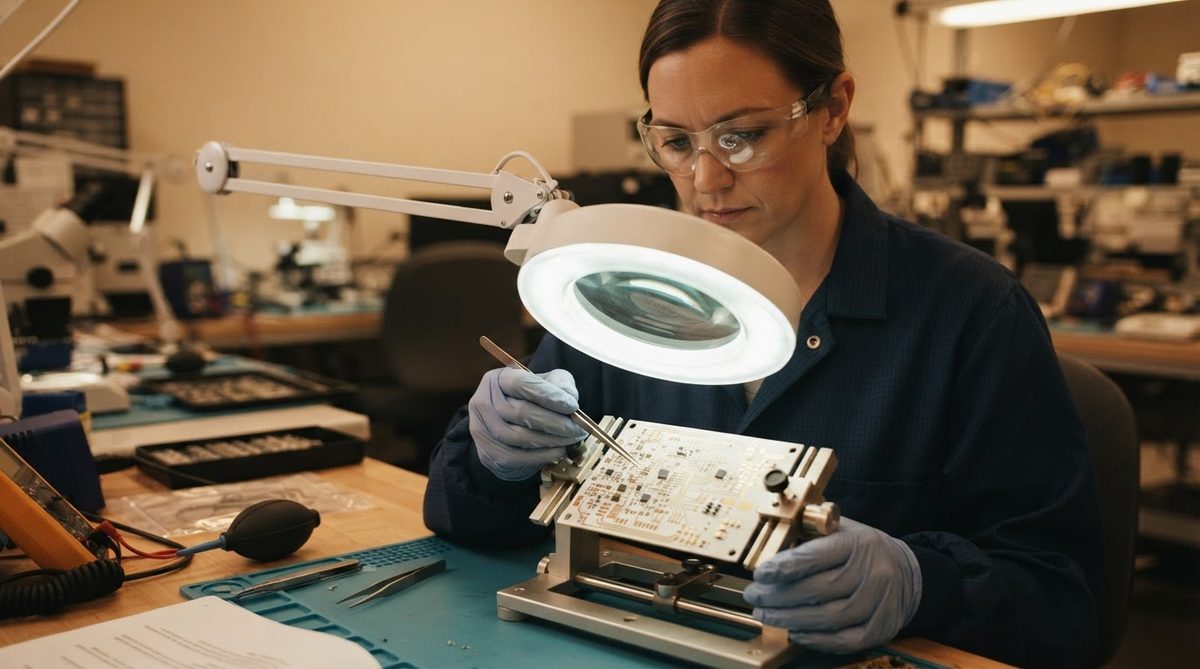
In the FR-4 world, a prototype is a handful of boards from a pooled panel. Ceramic prototyping works differently. Each substrate is individually processed, and there is no panel pooling across customers. Your prototype run ties up a furnace cycle, a metallization step, and often a laser or mechanical scribing tool—all for a small batch. That is why the per-piece cost for five ceramic boards can be 10–30× the unit cost you would pay at 1,000 pieces.
Prototypes serve three purposes that matter more for ceramic than for organic boards: verifying thermal performance against simulation, confirming solderability with your specific die-attach or reflow soldering profile for ceramic substrates, and checking dimensional fit in a mechanical assembly where CTE mismatch is a concern.
Material Options and Their Effect on Lead Time
Your substrate choice is the single largest variable in how fast you get boards back. Alumina (Al₂O₃) at 96% purity is the workhorse: blanks are widely stocked, and most ceramic PCB shops keep inventory on the shelf. Higher-purity 99.6% alumina is also commonly available but may add a day or two if the specific thickness you need is not in stock.
Aluminum nitride (AlN) and silicon nitride (Si₃N₄) substrates are specialty materials. Blanks are produced by fewer suppliers, carry longer raw-material lead times, and cost significantly more. Expect 10–15 business days for AlN and potentially longer for Si₃N₄, especially in non-standard thicknesses. If your project needs AlN or Si₃N₄ prototypes on a tight schedule, confirm blank availability before you finalize your design.
| Substrate | Typical Prototype Lead Time | Relative Unit Cost (vs. 96% Al₂O₃) | Notes |
|---|---|---|---|
| 96% Al₂O₃ | 5–10 business days | 1× | Blanks widely stocked |
| 99.6% Al₂O₃ | 7–12 business days | 1.5–2× | Check thickness availability |
| AlN | 10–15 business days | 3–5× | Fewer blank suppliers |
| Si₃N₄ | 12–18 business days | 5–8× | Limited stock, often made to order |
Lead times are shop-dependent and assume design files are production-ready at order entry. Expedite options may shorten these by 2–5 days at added cost.
Process Selection: DPC, DBC, Thick Film, or LTCC?
The metallization process determines your minimum feature size, copper thickness range, and which substrates you can use. For prototypes, this choice also affects cost and turnaround because each process has different tooling and setup overhead.
DPC (Direct Plated Copper)
DPC uses sputtering and photolithography to deposit and pattern copper on a ceramic substrate. It offers fine line/space capability (often down to 30–50 µm) and is well suited to high-density single- or double-sided prototypes on alumina or AlN. Setup cost is moderate because there is no custom screen or etching mask in the traditional sense—the pattern comes from a photomask generated directly from your Gerber files.
DBC (Direct Bonded Copper)
DBC bonds a pre-formed copper foil to the substrate at high temperature (around 1065 °C for Cu-Al₂O₃). It produces thick copper layers (typically 0.127–0.635 mm) suited to power electronics. DBC prototypes carry higher setup cost because each design needs a custom etching pattern on the bonded copper, and the bonding furnace cycle is time-consuming. Lead times are usually at the longer end of the ranges above.
Thick Film
Screen-printed conductors (Au, Ag, AgPd) fired at 850–1000 °C. Each layer needs a custom screen, which adds 1–3 days and a fixed cost per screen. For simple single-layer prototypes with moderate line widths (≥ 100 µm), thick film is cost-effective. For fine-pitch work, DPC wins.
LTCC
Low-temperature co-fired ceramic is the go-to for multilayer ceramic PCB builds. Prototyping LTCC is slower (often 15–25 days) because each layer requires screen printing, lamination, and co-firing. It is the right choice when you need embedded passives, hermetic cavities, or RF structures that cannot be achieved in two layers.
To review the full scope of available processes and spec limits, see the ceramic PCB manufacturing capabilities overview.
Worked Example: Prototype Cost Breakdown
Suppose you need 10 pieces of a 25 × 25 mm, double-sided DPC board on 96% Al₂O₃ (0.635 mm thick), with ENIG finish. Here is a representative cost structure:
| Cost Element | Estimated Range | Notes |
|---|---|---|
| Substrate blanks (10 pcs) | $15–$30 | Standard size, stocked |
| Photomask / tooling | $80–$150 | One-time, reusable for reorders |
| DPC metallization | $200–$400 | Sputtering + plating + etch |
| ENIG surface finish | $40–$80 | Batch process |
| Electrical test / QC | $30–$60 | Continuity, isolation, visual |
| Scribing / singulation | $20–$50 | Laser or diamond scribe |
| Total (10 pcs) | $385–$770 | $38–$77 per board |
These figures are illustrative. Actual pricing depends on the supplier, copper thickness, number of layers, and feature complexity. Request a quote for your specific design.
At 1,000 pieces, the tooling cost amortizes to nearly nothing, and the per-unit price might drop to $5–$12 for the same board. The steep prototype premium is almost entirely fixed-cost overhead spread across a tiny batch.
Design-for-Prototype Tips That Save Time
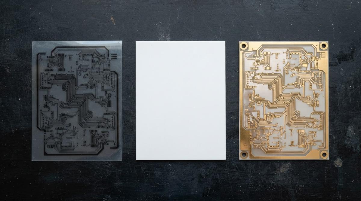
Most prototype delays happen before fabrication starts. The design file arrives, the manufacturer reviews it, finds issues, sends questions, and waits for answers. Each round-trip can cost 1–3 days. Eliminate the most common problems up front:
- Match your design rules to the process. If you are targeting DPC, confirm the shop’s minimum trace/space. Designing to FR-4 rules (e.g., 100 µm trace on a board that will be DBC with 300 µm minimum) guarantees a redesign cycle.
- Specify the substrate in your fab notes. State the material grade (e.g., “96% Al₂O₃ per Kyocera A-493”), thickness, and surface finish. “Ceramic” alone is not a specification.
- Account for shrinkage in LTCC. LTCC tapes shrink 12–16% during firing (per DuPont 951 datasheet, x-y shrinkage 12.7 ± 0.3%). Your Gerber must be pre-scaled, or the manufacturer must know to apply the scaling. Confirm who owns that step.
- Keep panelization simple. If your part is small, discuss array layout with the shop before submitting. Odd shapes or tight nesting wastes substrate and adds scribing time.
- Include a clear stackup drawing for multilayer builds. Layer count, dielectric thickness per layer, via type (filled, open, staggered), and conductor material for each layer.
For a deeper walkthrough of the fabrication sequence from Gerber to finished board, see the ceramic PCB manufacturing process guide.
When a Ceramic Prototype Is Not the Right Move
Ceramic prototypes make sense when the substrate’s thermal, dielectric, or mechanical properties are integral to the test you are running. They do not make sense in several common scenarios:
- You are only validating circuit function. If the prototype’s purpose is to check signal routing, firmware, or connector fit—and thermal performance is not yet critical—build on FR-4 or metal-core PCB first. You will get boards in 2–3 days at a fraction of the cost, and you can move to ceramic for the thermal validation round.
- Your design is still changing weekly. At $40–$80 per board for a small batch, iterating three or four times on ceramic gets expensive fast. Stabilize the schematic and layout on organic boards, then commit to a ceramic prototype.
- Volume pricing is the real question. If you need a ceramic prototype only to get a production quote, ask the manufacturer for a quote based on Gerber review without building samples. Most shops will provide a budgetary estimate from files alone.
Transitioning from Prototype to Production
A ceramic prototype built with one process (say, thick film) may not directly translate to a different production process (say, DPC). Line widths, registration tolerances, and conductor resistivity all change. Wherever possible, prototype on the same process you plan to use in production. This avoids a second qualification cycle and ensures your prototype test data is representative.
If you plan to rework or repair boards during prototype evaluation, understand the constraints. Ceramic substrates cannot be drilled or re-routed after firing. Read about repairing and reworking ceramic PCBs before you commit to a test plan that assumes easy modification.
FAQ
Can I order just one ceramic PCB prototype?
Yes. Most ceramic PCB manufacturers accept single-piece orders. The unit cost will be high because tooling and setup costs are spread across one board. Ordering 5–10 pieces is usually more cost-effective per unit and gives you spares for destructive testing or assembly trials.
Do I need different Gerber files for ceramic versus FR-4?
The file format is the same (RS-274X or Gerber X2), but your design rules will differ. Minimum trace/space, via sizes, and board outline tolerances are process-dependent. Always check the manufacturer’s design rules for the specific ceramic process before generating files.
Is expedited shipping worth it for ceramic prototypes?
Shipping time is rarely the bottleneck. A typical ceramic prototype spends 5–15 days in fabrication and 3–5 days in transit via air freight. Paying for overnight shipping saves 2–3 days at most. Investing in clean, error-free design files saves more calendar time than any shipping upgrade.
Can I reuse prototype tooling for production orders?
For DPC and thick-film processes, photomasks and screens created during prototyping are usually reusable for production runs of the same design. Confirm with your supplier whether tooling is retained and for how long. Some shops archive tooling for 6–12 months; others require a new setup fee after a period of inactivity.
What testing is typically done on ceramic prototypes?
Standard QC includes visual inspection under magnification, conductor continuity and isolation testing, and dimensional verification. Thermal cycling, wire-bond pull tests, or hipot testing are available on request but add cost and time. Specify your test requirements at order entry so they are included in the quoted lead time.
How do import tariffs affect ceramic prototype costs?
Ceramic PCBs imported into the U.S. from China may be subject to Section 301 tariffs. For small prototype quantities, the tariff amount per shipment is modest, but it adds to an already high per-unit cost. Review the details on tariffs and country of origin for ceramic PCB orders before budgeting.
Next Step
If you have Gerber files and a substrate preference ready, request a prototype quote to get exact pricing and lead time for your design. For general questions about ceramic PCB technology, the ceramic PCB FAQ covers 60+ common topics.