Ceramic PCB assembly uses the same pick-and-place and reflow equipment as FR-4 assembly, but the substrate’s brittleness, higher thermal mass, and tighter void-rate requirements force real changes to profiles, handling, and inspection. Skipping those changes leads to cracked boards, tombstoned passives, and die-attach voids that kill thermal performance. This guide covers what actually differs and how to get it right.
Key Takeaways
- Ceramic substrates (Al₂O₃, AlN, Si₃N₄) tolerate peak reflow temperatures above 300 °C, but thermal shock from fast ramps—not peak temperature—causes most assembly cracks.
- Recommended ramp rates for ceramic PCB reflow are 1–3 °C/s, roughly half the 3–5 °C/s common on FR-4 lines.
- Die-attach void rates below 5 % (per MIL-STD-883, Method 2030) are achievable with vacuum reflow or pressure sintering but require X-ray verification on every lot.
- Mechanical support tooling (vacuum nests or edge-rail pallets) is mandatory for substrates thinner than 0.5 mm to prevent fracture during conveyance.
- Solder paste selection matters more on ceramic than on FR-4 because the substrate’s near-zero moisture absorption changes flux activation behavior.
How Ceramic PCB Assembly Differs from FR-4 Assembly
FR-4 is a glass-epoxy laminate with a CTE of 14–17 ppm/°C in-plane. Alumina (Al₂O₃ 96 %) has a CTE of roughly 6.5–7.0 ppm/°C, and aluminum nitride (AlN) sits near 4.5 ppm/°C. That CTE mismatch between substrate and component leads means solder joints see higher shear stress during thermal cycling. It also means the reflow profile itself can induce enough differential expansion to crack a thin ceramic panel if the ramp is too steep.
The second difference is rigidity. FR-4 flexes; ceramic does not. A board that would survive a slight conveyor jam on an FR-4 line will snap on a ceramic line. Every touchpoint—stencil printer nest, pick-and-place support pins, reflow conveyor rails—must be reviewed for point loading. Flat vacuum nests distribute force evenly and are the standard approach for substrates under 0.5 mm thick.
Third, ceramic absorbs almost no moisture (water absorption < 0.01 % for 96 % alumina per CoorsTek datasheet). That eliminates the need for baking before reflow but also means flux solvents behave differently during preheat. Flux that activates correctly on a slightly moist FR-4 surface may under-activate on a bone-dry ceramic, leading to poor wetting. Choosing a flux designed for ceramic or noble-metal surfaces (ROL0 or ROL1 per IPC J-STD-004B) solves this.
SMT Process Steps on Ceramic Substrates
1. Solder Paste Printing
Use a laser-cut stainless steel stencil, 100–150 µm thick, matched to the pad geometry. Ceramic substrates are flatter than FR-4 (typical bow < 0.1 mm per 25 mm), so gasket sealing against the stencil is excellent. Snap-off distance can often be reduced to zero (contact printing), which improves paste release on fine-pitch pads below 0.4 mm.
For metallized ceramic (DPC or thick-film gold/silver), confirm solder paste compatibility with the surface finish. SAC305 (Sn96.5/Ag3.0/Cu0.5) wets well on nickel-gold and DPC copper with ENIG. High-lead solder (Pb93.5/Sn5/Ag1.5, liquidus ~305 °C) is still common in power modules and requires a dedicated high-temperature profile.
2. Component Placement
Standard pick-and-place machines handle ceramic boards if the conveyor is set up for the substrate dimensions. Ceramic PCB panels are often smaller than FR-4 panels—commonly 114 × 114 mm or 140 × 190 mm rather than the 457 × 610 mm standard. Check your machine’s minimum panel size and use ceramic panel size options that match your placement equipment’s rail width.
Nozzle touch-down force should be reduced 20–30 % below FR-4 defaults. A 0402 passive placed at 3 N touch-down on a 0.25 mm alumina substrate can initiate a micro-crack that propagates during reflow.
3. Reflow Soldering
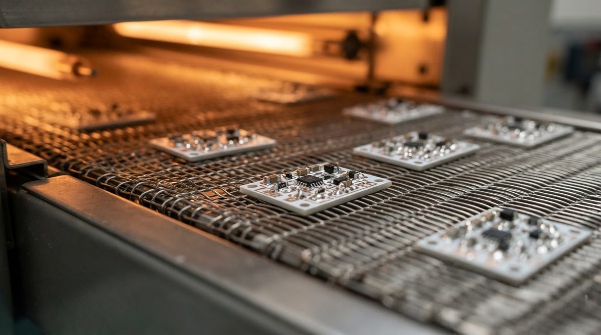
This is the step that breaks the most ceramic boards. The substrate’s thermal conductivity (24–28 W/mK for 96 % Al₂O₃, 170–200 W/mK for AlN) means it heats unevenly if only one side faces the heating element. Dual-sided heating (top and bottom IR or convection) is strongly preferred.
A typical SAC305 reflow profile tuned for ceramic substrates looks like this:
| Zone | Temperature Range | Duration | Ramp Rate |
|---|---|---|---|
| Preheat | 25–150 °C | 60–90 s | 1.0–1.5 °C/s |
| Soak | 150–200 °C | 60–120 s | 0.5–1.0 °C/s |
| Ramp to peak | 200–245 °C | 30–60 s | 1.0–2.0 °C/s |
| Time above liquidus (217 °C) | 217–245 °C | 40–70 s | — |
| Cooling | 245–100 °C | ≥ 60 s | ≤ 3.0 °C/s |
Profile targets for SAC305 on 96 % Al₂O₃, 0.38–0.63 mm thick. Confirm against your paste manufacturer’s datasheet and run a profiling board with thermocouples before production.
The cooling rate matters as much as the heating rate. Rapid cooling (> 4 °C/s) on a thin alumina substrate can cause thermal-shock fracture. Keep cooling at or below 3 °C/s through the solidification range.
Die Attach on Ceramic: Methods Compared
Power semiconductors, bare LEDs, and MEMS sensors are often mounted directly to ceramic substrates. The die-attach process on ceramic must form a low-thermal-resistance, mechanically reliable bond. Three methods dominate.
| Parameter | Solder Die Attach | Silver Sinter | Epoxy Die Attach |
|---|---|---|---|
| Bond-line thermal conductivity | 50–60 W/mK (SAC305) | 150–250 W/mK | 1–3 W/mK (Ag-filled) |
| Max operating temperature | ~200 °C (SAC), ~290 °C (high-Pb) | > 400 °C | 150–200 °C |
| Void rate (typical, with vacuum) | < 5 % | < 3 % | < 10 % |
| Process temperature | 240–320 °C | 230–280 °C + 10–30 MPa | 120–175 °C cure |
| Equipment cost | Moderate | High (press + oven) | Low |
| Rework feasibility | Yes, with local heating | Difficult | Chemical removal |
Typical values from Heraeus, Henkel, and Alpha Assembly Solutions datasheets. Confirm against your specific paste or preform.
Silver sintering delivers the best thermal path and is gaining ground in SiC and GaN power modules where junction temperatures exceed 200 °C. The trade-off is equipment cost and the difficulty of reworking or repairing ceramic assemblies after sintering. For prototyping and lower-power applications, solder die attach with vacuum reflow is the practical default.
Worked Example: Void-Rate Impact on Thermal Resistance
A 5 × 5 mm die is soldered to a DBC Al₂O₃ substrate with a 50 µm SAC305 bond line. The solder’s thermal conductivity is ~58 W/mK.
Thermal resistance of the bond line with 0 % voids: Rth = t / (k × A) = 0.00005 / (58 × 0.000025) = 0.034 °C/W.
At 20 % void rate, the effective contact area drops to 0.00002 m². Rth rises to 0.043 °C/W—a 26 % increase. For a 100 W die, that adds 0.9 °C to junction temperature. At 300 W (common in IGBT modules), it adds 2.7 °C—enough to eat into the thermal margin of a tightly designed system.
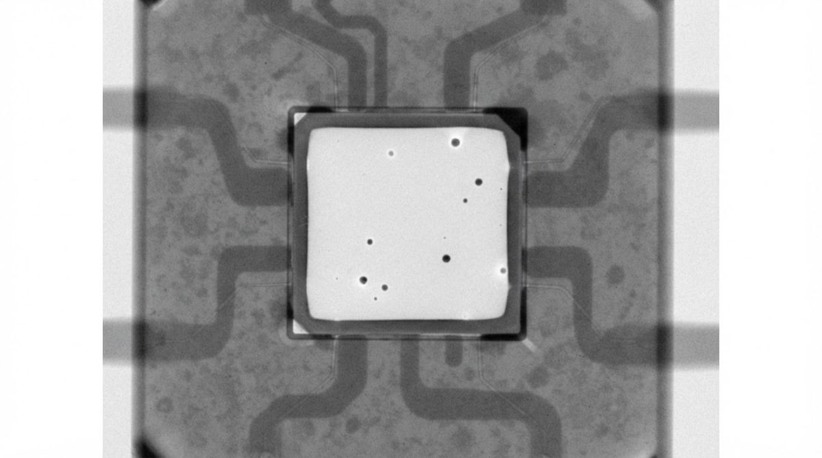
This is why X-ray inspection of die-attach voids is standard practice, not a nice-to-have, for power ceramic assemblies.
Handling and Conveyor Considerations
Ceramic substrates chip at edges and crack under point loads. Assembly lines need these adaptations:
- Edge handling: Use PEEK or Delrin edge guides, not bare stainless steel rails. Metal-on-ceramic contact during vibration causes edge chips.
- Vacuum nests: For substrates ≤ 0.38 mm thick, a flat aluminum vacuum nest supports the full underside during printing and placement.
- ESD trays: Store and transport boards in conductive waffle trays. Ceramic is an insulator; triboelectric charge builds up fast.
- No stacking: Never stack bare ceramic boards. Separate with anti-static interleave paper or individual slots in a cassette.
When Not to Use Ceramic PCB Assembly
Ceramic assembly adds cost and cycle time. It is the wrong choice when:
- Operating temperature stays below 130 °C and power density is moderate. FR-4 or metal-core PCB (MCPCB) handles this at a fraction of the cost.
- The board is large (> 150 × 150 mm) and densely populated. Large ceramic panels are expensive, fragile in conveyance, and hard to source. A hybrid approach—ceramic substrate for the power section, FR-4 for control logic—often works better.
- Flex or vibration tolerance is the primary concern. Ceramic is brittle. If the assembly will see repeated mechanical shock above ~50 g, consider polyimide flex or a mechanically decoupled mounting scheme.
- Prototype volume is very low and turnaround is critical. Ceramic substrate lead times are longer than FR-4. Check ceramic prototype turnaround options before committing to a schedule.
Frequently Asked Questions
Can I run ceramic boards through a standard SMT line?
Yes, most standard SMT lines can process ceramic boards with minor changes: slower conveyor speed, reduced nozzle force, and a modified reflow profile. The pick-and-place machine itself needs no hardware modification; the main adjustment is programming a gentler touch-down and ensuring the conveyor rail width accommodates the smaller panel.
Do I need a special solder paste for ceramic?
Not necessarily a special formulation, but you should use a flux classification suited to low-moisture surfaces (ROL0 or ROL1 per IPC J-STD-004B). Standard no-clean SAC305 paste works on ENIG or DPC copper finishes. For bare gold thick-film pads, an SnPb or AuSn eutectic paste may be required to avoid gold embrittlement.
What void rate is acceptable for die attach on ceramic?
For power applications, MIL-STD-883 Method 2030 sets a common benchmark of ≤ 5 % void area. Many automotive OEMs specify ≤ 2 % for SiC modules. Void rate is verified by X-ray inspection, and vacuum reflow or pressure sintering is typically needed to hit these targets consistently.
How do I prevent cracking during reflow?
Keep the heating ramp at or below 2 °C/s and the cooling ramp at or below 3 °C/s. Use dual-sided heating to minimize the temperature gradient across the substrate thickness. Support thin substrates (≤ 0.38 mm) on a flat carrier or vacuum nest throughout the reflow cycle.
Is ceramic PCB assembly more expensive than FR-4 assembly?
Assembly labor and machine time are similar, but total cost per board is higher because the substrate itself costs 5–20× more than FR-4, yield loss from cracking adds scrap cost, and inspection requirements (X-ray, void analysis) add process steps. The cost premium is justified when thermal or electrical performance cannot be met any other way.
Can I wave-solder through-hole components onto a ceramic board?
Wave soldering is possible but risky. The thermal shock of immersing a ceramic board in a 260 °C solder wave can crack thin substrates. Selective soldering with a programmable nozzle is safer because it limits the heated area. Most ceramic assemblies use only SMT and die attach, avoiding through-hole entirely.
Next Step
If you are planning a ceramic assembly, start by confirming your substrate material and understanding the full PCB manufacturing process from bare substrate through final test. Upload your design files for a quote and DFM review at AluminaPCB to get feedback on panel layout, pad design, and recommended reflow parameters before you commit to a production run.