How thin can ceramic PCB be in real production? Standard ceramic substrates reach 0.1 mm (100 µm) in both 96% alumina and aluminum nitride. Silicon nitride substrates go to 0.2 mm reliably. Going thinner is physically possible in a lab, but 0.1 mm is the practical floor for substrates that must survive scoring, shipping, pick-and-place, and reflow soldering in a real production environment.
Key Takeaways
- Standard thin ceramic substrates are produced at 0.25 mm, 0.38 mm, and 0.50 mm; ultra-thin grades reach 0.1 mm.
- Material choice sets the minimum: Al₂O₃ and AlN go to 0.1 mm; Si₃N₄ is practical at 0.2 mm due to different sintering behavior.
- Thinner substrates lower thermal resistance but reduce mechanical strength roughly with the square of thickness.
- Maximum unsupported panel size shrinks as thickness drops—a 0.1 mm alumina substrate is typically limited to about 50 × 50 mm.
How Thin Can Ceramic PCB Be by Material?
| Material | Practical Min Thickness | Common Thin Range | Flexural Strength (typical) | Source |
|---|---|---|---|---|
| Al₂O₃ 96% | 0.10 mm | 0.25–0.63 mm | 350–380 MPa (ASTM C1161) | CoorsTek ADS-96R datasheet |
| Al₂O₃ 99.6% | 0.10 mm | 0.25–0.50 mm | 380–450 MPa (ASTM C1161) | Kyocera A-493 datasheet |
| AlN | 0.10 mm | 0.25–0.63 mm | 300–350 MPa (ASTM C1161) | Maruwa AN-230 datasheet |
| Si₃N₄ | 0.20 mm | 0.32–0.63 mm | 700–850 MPa (ASTM C1161) | Kyocera SN-240 datasheet |
Typical values for commercially available material, for comparison only. Confirm against the datasheet for your specific grade.
For details on ultra-thin 99.6% alumina substrates, including standard stock sizes and tolerances, see the dedicated product page. Aluminum nitride thin substrates are covered separately on the AlN thin substrate page.
Why Thickness Matters: Thermal Resistance and Mechanical Strength
Thermal resistance through a substrate is directly proportional to thickness. Halving the substrate from 0.50 mm to 0.25 mm halves the conduction resistance. For a 10 × 10 mm die pad on 96% alumina (k ≈ 25 W/mK):
Worked example — thermal resistance through the substrate:
Rth = t / (k × A)
- At 0.50 mm: Rth = 0.0005 / (25 × 0.0001) = 0.20 °C/W
- At 0.25 mm: Rth = 0.00025 / (25 × 0.0001) = 0.10 °C/W
- At 0.10 mm: Rth = 0.0001 / (25 × 0.0001) = 0.04 °C/W
That 0.16 °C/W difference between 0.50 mm and 0.10 mm sounds small, but at 50 W dissipation it represents 8 °C of junction temperature. For high-power LEDs and RF transistors, that margin matters. Understanding how thin can ceramic PCB be for your application starts with this thermal calculation.
Enter your substrate area, thickness, and dissipated power below to estimate junction temperature rise for your own design.
The trade-off is mechanical. Flexural strength of a plate scales roughly with the square of its thickness for a given span. A 0.25 mm alumina substrate can withstand about one-quarter the bending load of a 0.50 mm substrate of the same grade. This is why silicon nitride, with roughly twice the flexural strength of alumina, is preferred for thin power-module substrates that undergo thermal cycling.
What Limits How Thin a Ceramic PCB Can Be
Sintering and Flatness
Ceramic substrates are made by tape-casting a green sheet and then sintering at 1,500–1,900 °C depending on the material. Thinner green sheets are harder to keep flat during sintering. Below 0.15 mm, camber (bow) can exceed 0.5% of the diagonal, which creates problems for die attach and wire bonding. Manufacturers control this with setter plates and controlled cooling profiles, but yields drop and cost rises.
Handling and Assembly
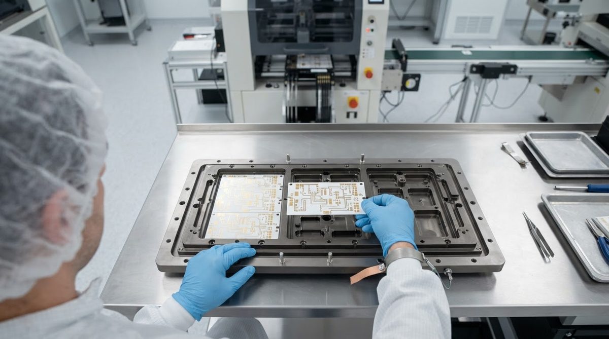
A 0.10 mm alumina substrate is fragile. It will survive automated pick-and-place if properly supported, but manual handling with tweezers risks edge chips. Most assembly houses require substrates to be delivered on carrier frames or dicing tape below 0.25 mm. Factor this into your assembly cost estimate.
Panel Size Constraints
Thinner substrates must be smaller. A 0.25 mm alumina panel can be produced at 100 × 100 mm or larger. At 0.10 mm, maximum practical panel size drops to roughly 50 × 50 mm for alumina and even smaller for AlN, which is more brittle. If your design needs a large board area, consider a multilayer ceramic build at a slightly greater thickness instead of pushing a single thin layer.
Via and Metallization Limits
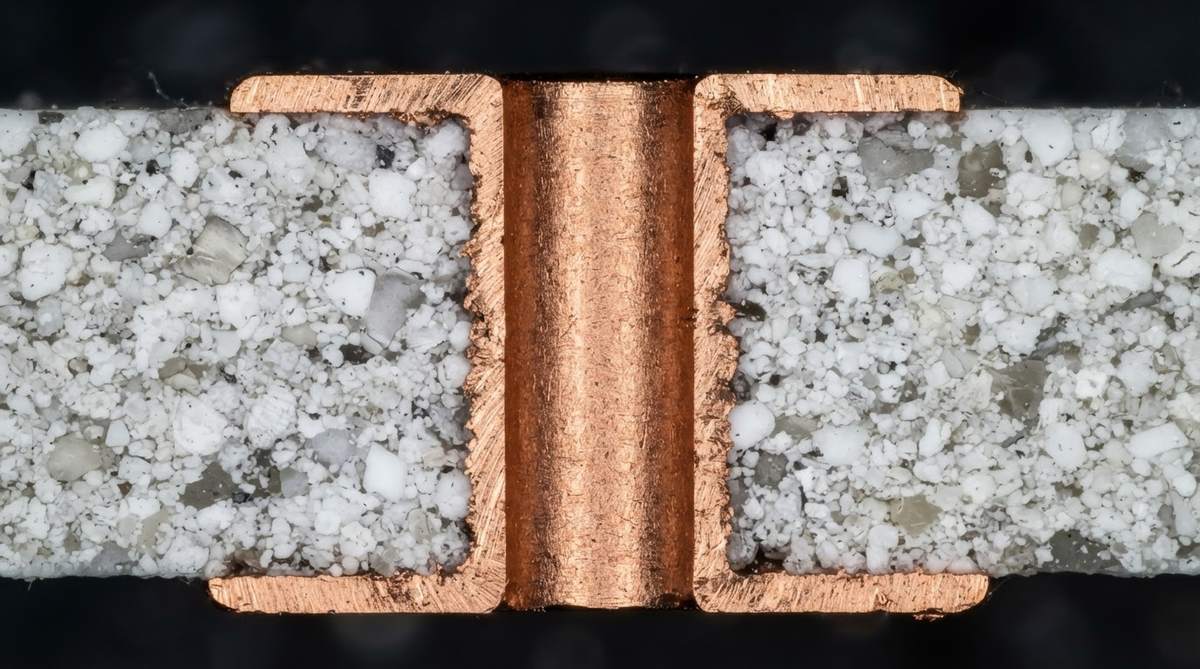
Thinner substrates restrict via diameter. A 0.25 mm substrate supports laser-drilled vias down to about 0.10 mm diameter. At 0.10 mm substrate thickness, via diameters of 0.05–0.08 mm are feasible with DPC (direct plated copper) processing, but aspect ratios below 1:1 are preferred to ensure reliable copper fill. Trace width and space are largely independent of substrate thickness, but registration accuracy can tighten because thinner substrates shift more during metallization.
When NOT to Use an Ultra-Thin Ceramic Substrate
Knowing how thin can ceramic PCB be is only half the question. Thin ceramic is the wrong choice when:
- Your board exceeds ~50 × 50 mm and must be unsupported. Use a standard 0.38 mm or 0.63 mm substrate, or switch to a metal-core PCB (MCPCB) for large-area LED arrays.
- The board will be hand-assembled or field-serviced. Substrates below 0.25 mm do not tolerate manual rework. FR-4 or standard-thickness ceramic is more practical.
- Thermal performance is not the driver. If your power density is low enough that 0.50 mm ceramic already meets your thermal budget, going thinner adds cost and fragility for no gain.
- You need through-hole components. Mechanical insertion stresses crack thin ceramic. Use 0.50 mm or thicker.
For a broader comparison of ceramic PCB fundamentals and when they make sense, start with the overview page.
Frequently Asked Questions
Can you get a ceramic PCB thinner than 0.1 mm?
Research labs have produced alumina films below 50 µm, but these are not practical as standalone PCB substrates. They lack the mechanical integrity for standard SMT assembly. For production boards, 0.1 mm is the realistic minimum for how thin can ceramic PCB be.
Does a thinner ceramic substrate cost more?
Yes. Substrates below 0.25 mm carry a premium of 20–50% over standard 0.63 mm grades, depending on material and quantity. The cost increase comes from lower sintering yields, tighter flatness screening, and special packaging for shipping.
Can I solder components directly onto a 0.1 mm ceramic substrate?
Yes, using reflow soldering with the substrate supported on a carrier or fixture. Vapor-phase reflow is preferred over convection for ultra-thin substrates because it applies heat more uniformly and reduces thermal shock risk. Avoid wave soldering entirely.
What is the thinnest silicon nitride substrate available?
Standard production Si₃N₄ substrates are available at 0.20 mm from manufacturers such as Kyocera and Toshiba Materials. Si₃N₄’s high fracture toughness (6–7 MPa·m½) makes it more handleable at thin gauges than alumina, but sintering costs keep it expensive. See the Si₃N₄ thin substrate page for specifications.
How do I specify thickness tolerance for a thin ceramic substrate?
Industry-standard tolerance for a 0.25 mm substrate is ±0.025 mm (±10%) per Kyocera and CoorsTek catalog specs. At 0.10 mm, expect ±0.015 mm. Always call out the tolerance on your drawing; “standard” varies by supplier.
Next Step
If your design calls for a substrate below 0.38 mm, send your layout and thermal requirements for a quick feasibility check. Thinner substrates often require material and panel-size adjustments early in the design phase. Request a quote through the ceramic PCB fabrication page to confirm lead time and available thicknesses for your material.