A sensor ceramic substrate PCB typically costs 3–15× more than an equivalent FR-4 board, with the exact multiplier set by three things: the ceramic material you choose, the minimum feature size your sensor layout demands, and your order volume. A 10 × 10 mm 96% alumina substrate with 100 µm traces in a run of 500 pieces might land at $2–$5 per unit, while the same footprint in aluminum nitride with 30 µm traces could reach $15–$40 per unit.
Key Takeaways
- 96% Al₂O₃ is the lowest-cost ceramic option for most sensor substrates, roughly $0.08–$0.15 per cm² in production volumes.
- Switching from alumina to AlN adds 3–5× to raw substrate cost but may be necessary for pyroelectric, thermopile, or high-frequency sensors.
- Trace/space below 50 µm usually requires thin-film metallization (sputtering + photolithography), which doubles or triples processing cost versus thick-film screen printing.
- Prototype runs of 5–25 pieces carry heavy NRE; amortizing tooling across 500+ pieces drops unit cost by 40–60%.
- Sensor substrates are small, so panel utilization is a hidden lever—fitting more units per firing panel cuts cost per piece significantly.
Material Choice Is the Biggest Cost Lever
The substrate itself accounts for 30–50% of total board cost at sensor-typical sizes (5 × 5 mm to 25 × 25 mm). Your material selection locks in a price floor before any metallization happens.
| Material | Relative substrate cost | Thermal conductivity (W/mK) | Typical sensor use |
|---|---|---|---|
| Al₂O₃ 96% | 1× | 24–28 (at 20 °C) | Pressure sensors, humidity sensors, general MEMS |
| Al₂O₃ 99.6% | 1.5–2× | 28–35 (at 20 °C) | High-frequency gas sensors, optical sensors |
| AlN | 3–5× | 170–200 (at 20 °C) | Thermopile IR sensors, pyroelectric detectors |
| LTCC (multilayer) | 2–4× (depends on layer count) | 2–3 (at 20 °C) | Integrated microfluidic sensors, RF sensor modules |
Typical values for commercially available material, for comparison only. Confirm against the datasheet for your specific grade. Thermal conductivity per CoorsTek and Kyocera published datasheets.
If your sensor operates below 150 °C and does not need sub-50 µm features, 96% alumina covers most requirements at the lowest cost. Reserve AlN for cases where thermal conductivity above 100 W/mK is a design requirement, not a preference. For a deeper look at AlN substrates for sensor applications, see our material-specific guide.
Metallization Process and Feature Size
Sensor layouts often need finer traces than power electronics. A resistive bridge for a pressure sensor might call for 50 µm lines; an interdigitated electrode for a gas sensor could need 20 µm fingers. The metallization process you need is dictated by these dimensions, and it directly sets processing cost.
- Thick film (screen printing): Minimum ~75–100 µm line/space. Lowest processing cost. One screen per layer, fired in a belt furnace. Suitable for RTD patterns, simple heater traces, and bond pads.
- Thin film (sputtering + photolithography): Down to 10–20 µm line/space. 2–3× the processing cost of thick film. Required for interdigitated electrodes, fine-pitch wirebond pads, and integrated thin-film resistors.
- DPC (direct plated copper): Typically 50–75 µm line/space. Mid-range cost. Good for sensor boards that need higher current-carrying capacity alongside moderate resolution.
A practical rule: if your design can live with 100 µm traces, thick film saves 40–60% on metallization compared to thin film. Redesigning an interdigitated electrode from 25 µm to 75 µm fingers—if the sensor physics allow it—can cut total board cost nearly in half.
Worked Cost Example: Piezoresistive Pressure Sensor Substrate
Consider a 10 × 10 mm, 0.38 mm thick 96% Al₂O₃ substrate with a Wheatstone bridge pattern (100 µm traces, thick-film Ag/Pd), ENIG finish on bond pads, and laser-scribed singulation from a 100 × 100 mm panel.
| Cost element | Estimated cost per piece (qty 500) | Notes |
|---|---|---|
| Raw substrate (panel, fired) | $0.60–$0.90 | ~100 units per panel; panel cost $60–$90 |
| Screen printing (2 layers) | $0.40–$0.70 | Paste + firing; screen amortized over run |
| ENIG finish | $0.15–$0.25 | Pad-only selective plating |
| Laser singulation | $0.20–$0.35 | CO₂ or Nd:YAG, depends on kerf tolerance |
| Electrical test / visual inspection | $0.10–$0.15 | Continuity + isolation check |
| Total per piece | $1.45–$2.35 |
Estimates based on typical contract manufacturing pricing for 96% Al₂O₃ thick-film substrates. Actual quotes vary by supplier and region.
At quantity 25 (prototype), expect $8–$15 per piece for the same design due to NRE for screens and setup. This is where understanding ceramic PCB cost factors helps you plan budgets across development stages.
Panel Utilization: A Cost Lever Unique to Small Sensor Boards
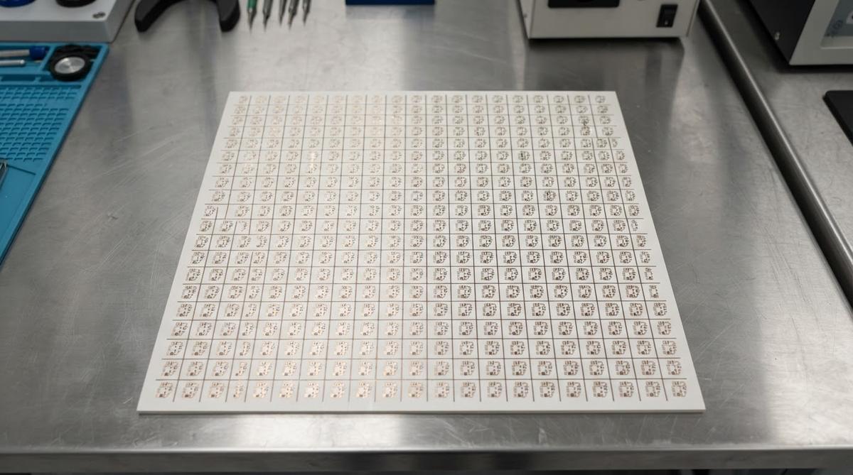
Sensor substrates are often tiny—5 × 5 mm or 8 × 12 mm. A standard 114 × 114 mm ceramic panel can hold dozens or even hundreds of units. The more units per panel, the lower your cost per piece, because firing, printing, and handling costs are per-panel, not per-unit.
If your design is 7 × 7 mm, fitting it onto a 4.5″ × 4.5″ panel yields roughly 196 units (14 × 14 grid with 0.5 mm streets). Shrinking the singulation street from 0.5 mm to 0.3 mm adds ~15% more units per panel. Discuss panel layout with your fabricator early—it is free optimization.
When NOT to Use a Ceramic Substrate for Your Sensor
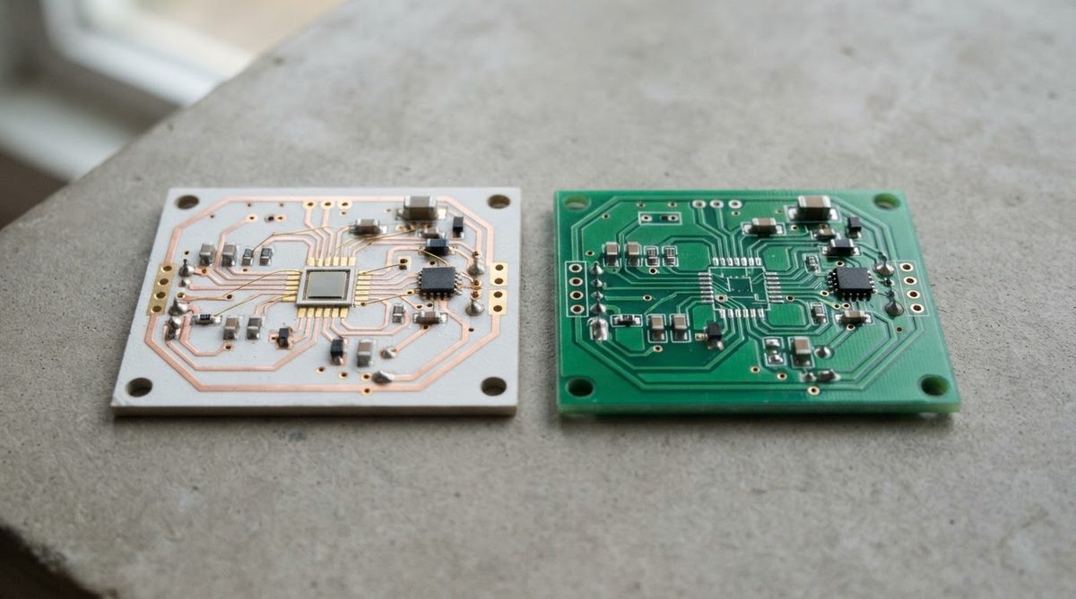
Ceramic is not always the right call. Choose FR-4 or flex if your sensor operates below 125 °C, needs no hermetic sealing, tolerates CTE mismatch with a polymer substrate, and has traces above 100 µm. A consumer humidity sensor on FR-4 costs $0.10–$0.30 per board at volume—an order of magnitude less than ceramic.
Metal-core PCBs (MCPCBs) suit sensors that need good thermal spreading but not electrical isolation at high temperatures. If your sensor is a simple thermistor interface board running below 150 °C, MCPCB is cheaper and easier to source.
For cost comparisons with other ceramic application types, see our guides on UV LED ceramic PCB cost and SiC power module substrate pricing.
How to Reduce Sensor Ceramic PCB Cost Without Sacrificing Performance
- Use 96% alumina unless your spec sheet demands otherwise. It covers >70% of sensor substrate applications.
- Design to thick-film rules (≥100 µm trace/space) where sensor physics allow.
- Maximize panel utilization. Provide your fabricator with a panel layout suggestion, not just a single-unit Gerber.
- Consolidate prototype and production orders. Running 500 pieces instead of two batches of 250 saves one setup charge.
- Specify only the finish you need. Bare gold wirebond pads cost less than full-board ENIG.
Enter your substrate dimensions, material, and quantity below to get a ballpark sensor ceramic substrate PCB cost estimate.
[pcb_calc type=”pcb-quote”]
Preparing an Accurate Quote Request
To get a tight quote rather than a wide range, send your fabricator a complete data package. Our guide on what to send for an accurate ceramic PCB quote lists every file and spec you should include. At minimum: Gerber or DXF files, substrate material and thickness, metallization type, surface finish, quantity, and any special testing requirements (hermeticity, hi-pot, etc.).
Frequently Asked Questions
How much does a single prototype sensor ceramic PCB cost?
A single 96% alumina sensor substrate with thick-film metallization typically costs $8–$20 per piece at quantities of 5–25, depending on size and complexity. NRE charges for screen fabrication and setup add $100–$300 per design. These fixed costs dominate at low volumes.
Is LTCC more expensive than single-layer alumina for sensors?
Yes. LTCC multilayer substrates cost 2–4× more than single-layer 96% alumina, mainly due to tape casting, via filling, lamination, and co-firing steps. LTCC makes sense when you need embedded passives, microfluidic channels, or integrated RF structures that would otherwise require separate components.
Can I use the same ceramic substrate for both the sensor element and the readout circuit?
You can, and doing so often reduces total system cost by eliminating a separate PCB and interconnect. Thick-film resistors for bridge circuits and thin-film conductors for signal routing can coexist on one alumina substrate, though you may need a hybrid metallization process that adds cost per piece.
Does gold metallization add a lot to sensor substrate cost?
Gold thick-film paste is roughly 5–8× the cost of silver or silver-palladium paste per gram. On a small sensor substrate (10 × 10 mm), the gold material cost adds $0.30–$1.00 per piece. The real cost impact comes if you need gold on large areas rather than just wirebond pads—keep gold coverage to the minimum your bonding process requires.
What volume makes ceramic sensor substrates cost-competitive with hybrid alternatives?
NRE amortization flattens out around 500–1,000 pieces for thick-film processes. Above 1,000 units, the per-piece cost stabilizes and further savings come mainly from material negotiations and panel utilization improvements. Thin-film processes need higher volumes—typically 2,000+ pieces—before NRE becomes negligible.