A ceramic PCB for a UV or UV-C LED array typically costs 3–8× more than an equivalent aluminum MCPCB. Understanding UV LED PCB PCB cost starts with the numbers: single-unit prices range from roughly $15–$80 for a 25 × 25 mm board depending on substrate material, metallization method, and surface finish. The premium exists because UV-C wavelengths (200–280 nm) degrade organic-based substrates within hundreds of hours, making alumina or aluminum nitride the only reliable long-term choices.
Key Takeaways
- 96% alumina (Al₂O₃) is the default substrate for UV LEDs emitting above 300 nm; AlN is preferred below 280 nm where thermal density exceeds ~25 W/cm².
- Substrate material accounts for 30–50% of total board cost; AlN substrates cost 4–6× more than 96% alumina per unit area.
- Reflective silver or aluminum mirror layers add 10–20% to fabrication cost but can increase UV-C optical output by 15–30%.
- Panelization and standardizing to common substrate sizes can reduce per-board cost by 20–40%.
- Metal-core PCBs fail in UV-C applications because the solder mask and dielectric yellow and crack under prolonged short-wavelength exposure.
Why UV and UV-C LEDs Need Ceramic Substrates
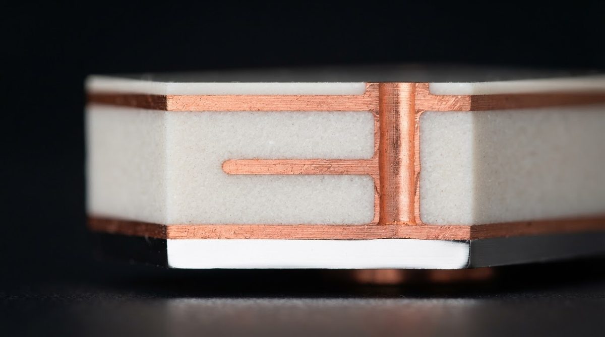
UV-C LEDs, particularly those in the 265–275 nm germicidal band, generate intense photon energy that breaks C–C and C–O bonds in organic polymers. FR-4 epoxy, polyimide flex, and the filled-polymer dielectrics used in MCPCBs all degrade under this radiation. Yellowing starts within 500–1,000 hours; delamination and cracking follow. Ceramic substrates—alumina, AlN, and occasionally 99.6% alumina—are inorganic and completely immune to UV photodegradation.
Thermal management matters equally. A single UV-C LED die dissipates 1–3 W in a footprint under 2 × 2 mm, with wall-plug efficiencies of only 3–10% (per Nichia NCSU334B datasheet). That means 90–97% of input power becomes heat. Alumina at 24–28 W/m·K handles moderate arrays; AlN at 170–200 W/m·K is necessary for tightly packed multi-die modules where junction temperature must stay below 80 °C to preserve UV-C output and lifetime.
Five Biggest UV LED PCB PCB Cost Drivers
1. Substrate Material Selection
Material is the single largest lever affecting UV LED PCB PCB cost. For a 25 × 25 mm substrate at 0.635 mm thickness, expect roughly $2–$4 for 96% Al₂O₃, $5–$8 for 99.6% Al₂O₃, and $12–$22 for AlN. The choice depends on thermal load per die and required optical reflectance at the target wavelength. Many UV-A (365 nm) curing applications work fine on 96% alumina; germicidal UV-C arrays with junction temperatures above 100 °C need AlN.
2. Metallization Process
DPC (direct plated copper) and thin-film sputtering deliver the fine features UV LED footprints require—trace/space down to 30–50 µm. Thick-film screen printing is cheaper but limited to ~100 µm lines. DPC adds roughly $8–$15 per board in small quantities versus $3–$6 for thick film. If your LED pitch is 3 mm or wider, thick film is sufficient and saves 30–50% on metallization cost.
3. Reflective Mirror Layer
UV LED boards often include a high-reflectance layer beneath and around the die to redirect downward and lateral photons upward. Silver mirrors reflect >95% above 350 nm but drop below 50% at 265 nm. Aluminum mirrors maintain >80% reflectance down to 250 nm (per CoorsTek UV substrate application note). Adding a sputtered aluminum mirror layer with a protective SiO₂ overcoat typically adds 10–20% to fabrication cost but can boost module optical output by 15–30%, improving system-level cost per milliwatt.
4. Surface Finish and Solder Pad Plating
Standard ENIG works for most UV LED soldering. For UV-C boards where the finish is directly exposed to radiation, gold plating thickness may need to increase to 0.05–0.1 µm to prevent nickel migration and tarnishing. Thicker gold adds $1–$3 per board. Some designs use bare silver pads with a conformal SiO₂ passivation layer instead, which costs slightly more but doubles as part of the mirror structure.
5. Board Size and Panelization
Ceramic substrates are processed on fixed panel sizes. A 25 × 25 mm board cut from a 114 × 114 mm (4.5″) panel yields 16 units. A 30 × 30 mm board yields only 9 from the same panel—44% fewer boards with roughly the same processing cost. Designing to panel-friendly dimensions is the simplest way to reduce your ceramic PCB cost.
Cost Comparison: Ceramic vs. MCPCB vs. FR-4 for UV LEDs
| Parameter | 96% Al₂O₃ (DPC) | AlN (DPC) | Aluminum MCPCB | FR-4 |
|---|---|---|---|---|
| Substrate cost (25 × 25 mm) | $18–$35 | $40–$80 | $3–$8 | $1–$3 |
| Thermal conductivity (W/m·K) | 24–28 | 170–200 | 1–3 (dielectric layer) | 0.3 |
| UV-C stability (>5,000 h) | Yes | Yes | No—dielectric degrades | No—epoxy yellows |
| Reflectance at 265 nm (with Al mirror) | >80% | >80% | N/A | N/A |
| Min trace/space | 30–50 µm | 30–50 µm | 75–100 µm | 75–100 µm |
| Typical lead time (prototype) | 2–3 weeks | 3–4 weeks | 1–2 weeks | 3–5 days |
Typical values for commercially available material, for comparison only. Confirm against the datasheet for your specific grade.
Worked Example: UV LED PCB PCB Cost per Milliwatt for a Germicidal Module
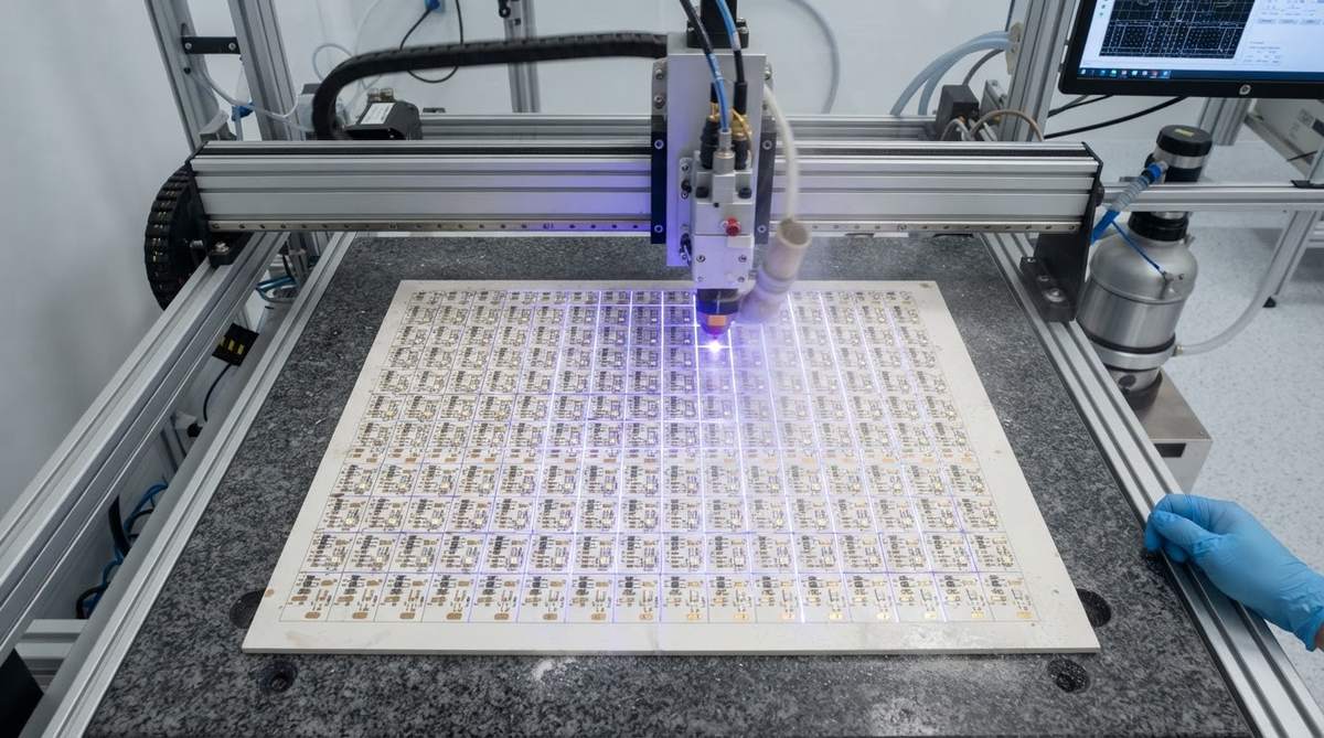
Consider a 4-die UV-C module (265 nm, 70 mW per die at 350 mA) on a 20 × 20 mm substrate.
- Option A — 96% Al₂O₃ with DPC + Al mirror: Board cost ~$25. Total optical output ~280 mW. Board cost per mW: $0.089.
- Option B — AlN with DPC + Al mirror: Board cost ~$55. Junction temperature drops ~15 °C, boosting per-die output to ~80 mW (per Nichia derating data). Total output ~320 mW. Board cost per mW: $0.172.
- Option C — Aluminum MCPCB (UV-A only, shown for reference): Board cost ~$5. UV-C degradation makes this unsuitable beyond ~1,000 hours. Not viable for germicidal use.
For this module, 96% alumina delivers the lowest UV LED PCB PCB cost per milliwatt. AlN becomes worthwhile only when the array density increases or when the thermal budget demands junction temperatures below 60 °C for extended lifetime targets (>20,000 h). Comparing high-power LED ceramic board pricing shows similar trade-offs in visible-light high-flux designs.
Enter your substrate dimensions, LED count, and target wavelength below to get a ballpark UV LED PCB PCB cost estimate for your project.
[pcb_calc type=”pcb-quote”]
When NOT to Use a Ceramic PCB for UV LEDs
UV-A (365–405 nm) at low power density. If each LED dissipates under 0.5 W and the array is spaced at ≥5 mm pitch, an aluminum MCPCB with a UV-stable white solder mask may last 10,000+ hours at a fraction of ceramic cost. Test coupon aging under your actual irradiance before committing.
Disposable or short-life products. Some consumer UV-C wands target only 2,000–3,000 hours of life. An MCPCB may survive long enough, making the ceramic premium unnecessary.
Very large boards (>150 × 150 mm). Ceramic substrates are limited in panel size and become prohibitively expensive at large dimensions. For large-area UV curing systems, consider tiling multiple small ceramic sub-modules onto an aluminum heat sink instead of one monolithic board.
Applications in aerospace and defense ceramic PCBs or medical device ceramic boards share similar cost-versus-reliability calculations.
FAQ
Can I use standard solder paste on a UV LED ceramic PCB?
Yes. SAC305 or AuSn solder pastes work on ceramic UV LED boards with ENIG or gold-plated pads. Reflow profiles follow the same curves as any ceramic assembly—typically 30–60 s above liquidus at 240–260 °C for SAC305. The ceramic substrate’s low CTE (6.5–7.0 ppm/°C for alumina) closely matches the AlGaN LED die (~5.6 ppm/°C), reducing solder joint stress.
Does the ceramic substrate itself reflect UV-C light?
Bare 96% alumina reflects roughly 60–70% of 265 nm light, which is moderate but not optimal. A sputtered aluminum mirror with SiO₂ passivation raises reflectance above 80% at 265 nm. AlN without a mirror reflects only ~40% at that wavelength due to its darker body color. The mirror layer is what matters, not the substrate choice alone.
How long does a ceramic UV-C LED board last compared to MCPCB?
Ceramic substrates show no measurable degradation after 50,000+ hours of UV-C exposure in accelerated aging tests. MCPCBs with polymer dielectrics typically begin to yellow and lose reflectance within 1,000–3,000 hours under direct 265 nm irradiation at power densities above 50 mW/cm². The failure mode is dielectric cracking, which can cause electrical shorts.
What is the minimum order for UV LED ceramic PCB prototypes?
Most ceramic PCB fabricators accept orders as low as 1–5 pieces for prototypes. Lead times for DPC on alumina prototypes run 2–3 weeks. AlN prototypes may take 3–4 weeks due to more limited raw material availability. See the ceramic PCB pricing guide for typical cost ranges.
Is AlN always better than alumina for UV-C LEDs?
No. AlN is thermally superior (170–200 W/m·K vs. 24–28 W/m·K) but costs 4–6× more. For arrays with fewer than 8 dies at moderate drive currents (≤350 mA per die), 96% alumina keeps junction temperatures within safe limits and delivers a lower cost per milliwatt. AlN pays off when thermal density exceeds roughly 25 W/cm² or when lifetime targets demand junction temperatures below 60 °C.