A single ceramic laser diode submount costs roughly $0.80–$6.00 in production volumes of 1,000–10,000 pieces, with aluminum nitride (AlN) submounts at the upper end and 96% alumina (Al₂O₃) at the lower end. Understanding laser diode submount PCB cost starts with four variables you can control at the design stage: substrate material, metallization stack, dimensional tolerances, and surface finish.
Key Takeaways
- AlN submounts cost 3–5× more than 96% alumina submounts of the same geometry, driven by raw material and processing costs.
- Tight positional tolerances (±25 µm or below) for die-attach pads can add 15–30% to unit cost due to photolithographic metallization requirements.
- Gold (Au) metallization—standard for laser diode submounts—accounts for 20–40% of total unit cost at current Au prices (~$75/g as of mid-2025).
- Prototype runs of 25–100 submounts typically cost 8–15× the production unit price because tooling and setup costs are amortized over fewer parts.
- Switching from a full-gold top layer to a selective Au pattern on Ni/Ti can cut metallization cost by 30–50%.
Why Laser Diode Submounts Need Ceramic
A laser diode chip dissipates 1–15 W from a footprint often smaller than 1 mm × 0.5 mm. That heat flux can exceed 1 kW/cm². FR-4 (0.3 W/mK) and even metal-core PCBs (1–3 W/mK) cannot move heat away fast enough to keep the junction below its rated limit, which is typically 60–85 °C for telecom-grade lasers.
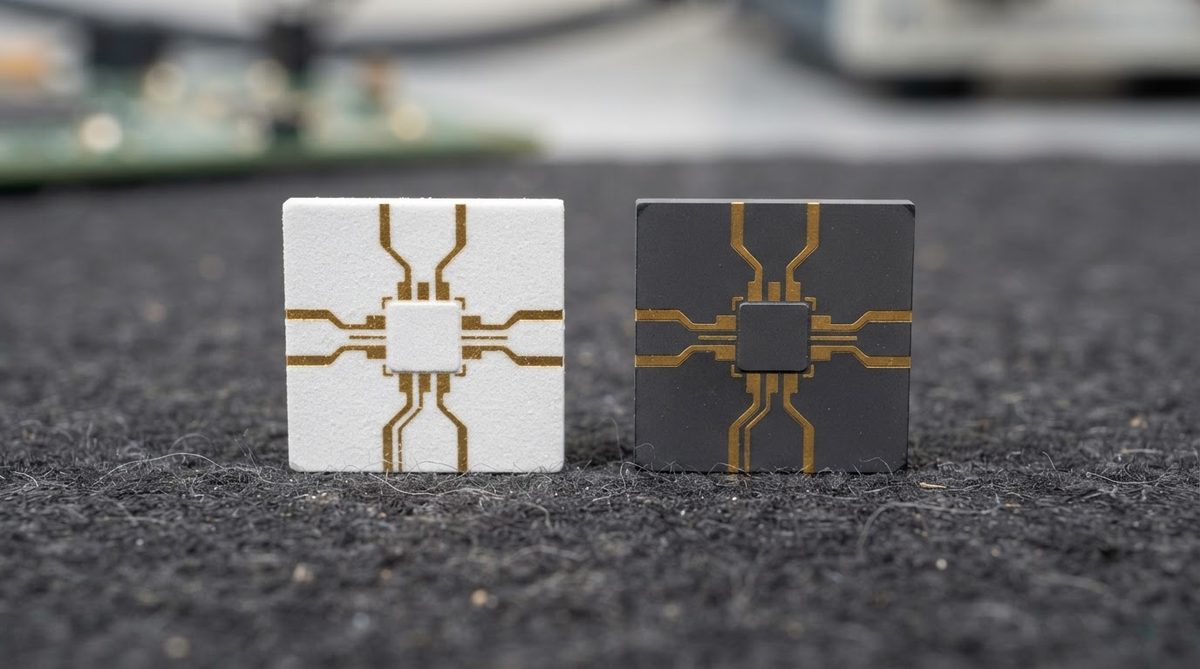
Ceramic substrates bridge the gap. AlN at 170–200 W/mK (per Kyocera SH-30 datasheet, measured at 20 °C) provides thermal conductivity close to copper, while also offering a coefficient of thermal expansion (CTE) of 4.5–4.7 ppm/°C—closely matching GaAs (5.7 ppm/°C) and InP (4.6 ppm/°C) die materials. That CTE match is critical: it reduces solder joint stress during thermal cycling and extends device lifetime. Alumina at 24–28 W/mK works for lower-power VCSELs and photodiodes where heat flux is more moderate. These thermal properties are a major reason the ceramic thermal management approach dominates photonics packaging.
What Drives Laser Diode Submount PCB Cost
1. Substrate Material
Material selection is the single largest cost lever. AlN substrates cost $0.40–$1.50 per cm² depending on thickness (typically 0.25–0.635 mm for submounts), while 96% alumina runs $0.08–$0.25 per cm². For a 2 mm × 2 mm submount, the raw substrate cost difference is small in absolute terms, but it scales quickly at volumes above 10k. For a full breakdown of how material choice affects ceramic board pricing, see the ceramic PCB cost breakdown.
2. Metallization Stack and Gold Content
Most laser submounts require a Ti/Pt/Au or Ti/Ni/Au metallization stack for reliable AuSn eutectic die attach. The gold layer alone—typically 1–5 µm thick—dominates metallization cost. A 2 mm × 2 mm pad with 3 µm Au uses roughly 0.0023 g of gold per side. At $75/g, that is $0.17 per pad, per side. For a submount with patterned top and blanket bottom metallization, gold cost per unit can reach $0.50–$1.20.
Thin-film sputtering (Ti/Pt/Au) gives tighter pattern definition (±10 µm) but costs more per run than thick-film screen printing. If your design allows ±50 µm pad tolerances, thick-film metallization can reduce processing cost by 20–35%.
3. Dimensional and Positional Tolerances
Standard dicing tolerance for ceramic submounts is ±50 µm. Laser packaging often demands ±25 µm or tighter for passive alignment to fiber arrays. Achieving this requires laser-cut or precision-diced singulation and 100% dimensional inspection, adding $0.10–$0.30 per unit.
4. Surface Finish and Flatness
Solder wetting and die-attach voiding depend on surface roughness. A lapped and polished AlN surface (Ra < 0.1 µm) costs significantly more than an as-fired surface (Ra 0.3–0.8 µm). If your die-attach process tolerates Ra 0.2–0.4 µm, specifying a lapped-only finish instead of polish can save 10–20% on substrate preparation.
5. Volume and NRE
Photomask tooling for thin-film metallization runs $500–$2,000 per layer. At 100 pieces, that adds $5–$20 per unit. At 10,000 pieces, it becomes negligible. Understanding tooling and NRE costs for ceramic PCBs helps you plan prototype budgets accurately.
Worked Example: AlN Submount Cost at 5,000 Units
Consider a 3 mm × 3 mm × 0.5 mm AlN submount with Ti/Pt/Au top metallization (3 µm Au, patterned), blanket Au bottom, ±25 µm dicing tolerance, and lapped surface finish. This example illustrates how each element contributes to total laser diode submount PCB cost.
| Cost Element | Estimate per Unit | Notes |
|---|---|---|
| AlN substrate (diced) | $0.60–$0.90 | 0.09 cm², lapped, ±25 µm dicing |
| Top metallization (Ti/Pt/Au, thin film) | $0.80–$1.20 | Includes 3 µm Au, photolithography |
| Bottom metallization (blanket Au) | $0.30–$0.50 | No patterning needed |
| NRE (amortized) | $0.15–$0.30 | Photomask + setup over 5,000 pcs |
| Inspection and packing | $0.10–$0.20 | 100% dimensional check, waffle tray |
| Total | $1.95–$3.10 | FOB, excluding shipping |
Typical values for comparison only. Confirm against your specific grade and supplier quotation.
Upload your submount design files to get a project-specific price estimate within hours.
[pcb_calc type=”pcb-quote”]
Comparison: Alumina vs. AlN Submount Costs and Performance
| Parameter | Al₂O₃ 96% | AlN | Unit | Condition | Source |
|---|---|---|---|---|---|
| Thermal conductivity | 24–28 | 170–200 | W/mK | 20 °C | Kyocera A-493, SH-30 datasheets |
| CTE | 7.1–7.4 | 4.5–4.7 | ppm/°C | 20–400 °C | CoorsTek ADS-996, Kyocera SH-30 |
| Dielectric strength | 10–15 | 14–17 | kV/mm | 25 °C, per ASTM D149 | Maruwa datasheets |
| Typical unit cost (3 × 3 mm, 5k qty) | $0.80–$1.60 | $1.95–$3.10 | USD | Ti/Pt/Au both sides | Industry estimates, mid-2025 |
| CTE match to GaAs (5.7 ppm/°C) | Fair | Good | — | — | — |
| CTE match to InP (4.6 ppm/°C) | Poor | Excellent | — | — | — |
Typical values for commercially available material, for comparison only. Confirm against the datasheet for your specific grade.
For lower-power photonics applications like VCSEL arrays or monitor photodiodes dissipating under 0.5 W, alumina submounts offer adequate thermal performance at roughly half the cost of AlN. The cost picture for semiconductor packaging ceramic PCBs follows similar material-driven patterns.
How to Reduce Laser Diode Submount PCB Cost
- Panelize aggressively. Submounts are small. A 100 mm × 100 mm AlN panel can yield over 1,000 units at 3 × 3 mm. Larger panels amortize metallization and handling costs more effectively.
- Minimize gold area. Pattern Au only where solder wetting is required. Leave non-functional areas unplated or use Ni as the top layer.
- Relax tolerances where possible. If active alignment is part of your packaging flow, ±50 µm dicing may be acceptable, saving 15–25% versus ±25 µm.
- Use alumina for low-flux devices. A VCSEL emitting 0.2 W from a 250 µm aperture generates far less thermal stress than a 10 W pump laser. Match the substrate to the actual heat load.
- Consolidate orders. Combining prototype and first-production runs reduces the number of NRE charges. A ceramic PCB prototype cost guide explains how to structure this.
When Not to Use a Ceramic Submount
Ceramic submounts add cost and lead time. They are not always necessary. Consider alternatives in these cases:
- Low-power, low-duty-cycle lasers (< 0.1 W average): A copper or CuW submount with direct solder may be simpler and cheaper, especially if CTE match is less critical (e.g., large die with compliant solder).
- Non-hermetic consumer modules: If the module is not hermetically sealed and lifetime requirements are under 5,000 hours, an aluminum metal-core PCB at $0.10–$0.30 per unit may suffice for the thermal load.
- Very high volume (>1M units) with relaxed thermal specs: Silicon submounts fabricated on standard wafer lines can undercut ceramic on laser diode submount PCB cost at extreme scale, though thermal conductivity (148 W/mK) is lower than AlN.
For applications in adjacent industries, the UV LED ceramic PCB cost analysis covers similar trade-offs for optoelectronic devices on ceramic.
Frequently Asked Questions
Can I use alumina instead of AlN for a 5 W laser diode?
Generally no. A 5 W laser diode on a 2 mm × 2 mm footprint produces a heat flux around 125 W/cm². Alumina’s 24–28 W/mK thermal conductivity creates a thermal resistance roughly 6–7× higher than AlN for the same geometry, which typically pushes junction temperature beyond safe limits. AlN is the standard choice above about 1–2 W for edge-emitting laser diodes.
What is the minimum order quantity for laser diode submounts?
Most ceramic PCB manufacturers accept orders starting at 25–100 pieces for prototypes. Production MOQs vary but commonly start at 500–1,000 units. Smaller quantities are feasible but carry higher per-unit costs because NRE and setup charges are spread across fewer parts.
Does solder preform add to submount cost?
Yes. Pre-deposited AuSn solder (typically 3–5 µm by evaporation or sputtering) adds $0.20–$0.60 per unit depending on area and deposition method. Using a separate solder preform placed during assembly shifts that cost to your packaging step but avoids the deposition charge on the submount itself.
How does gold price volatility affect submount pricing?
Gold accounts for 20–40% of a typical AlN submount’s cost. A 10% swing in gold spot price translates to roughly a 2–4% change in finished submount price. Most suppliers quote with a gold price validity window of 7–14 days. Locking in material early or reducing Au layer thickness from 5 µm to 2 µm (where your solder process allows) are the most effective hedges.
What lead time should I expect for ceramic laser submounts?
Prototype submounts (thin-film metallized AlN) typically ship in 3–5 weeks. Production orders at 5,000+ units take 4–8 weeks depending on metallization complexity and inspection requirements. Panelized designs with standard metallization stacks ship faster than custom geometries requiring new photomasks.