Introduction to PCB manufacturing
Printed Circuit Boards (PCBs) are essential components in modern electronics. They provide a platform for mounting and connecting electronic components, allowing for the creation of complex circuits in a compact and efficient manner. This tutorial will guide you through the process of PCB manufacturing, from designing your circuit to the final assembly.
What is a PCB?
A PCB is a thin board made of insulating material, such as fiberglass or composite epoxy, with conductive copper traces etched onto its surface. These traces connect the various components of an electronic circuit, such as resistors, capacitors, and integrated circuits (ICs). PCBs come in various sizes and can have multiple layers, depending on the complexity of the circuit.
Advantages of using PCBs
- Compact design
- Efficient and reliable connections
- Reduced wiring errors
- Easier to mass-produce
- Improved circuit performance
PCB Design Process
Schematic design
The first step in creating a PCB is to design the schematic of your electronic circuit. A schematic is a diagram that shows the interconnections between the various components in your circuit. You can use electronic design automation (EDA) software, such as KiCad or Eagle, to create your schematic.
PCB layout design
Once your schematic is complete, you need to create the PCB layout. The layout determines the physical placement of components and the routing of the copper traces on the board. When designing your PCB layout, consider the following factors:
- Component placement for optimal performance and ease of assembly
- Trace width and spacing to minimize electromagnetic interference (EMI)
- Ground planes and power planes for improved signal integrity
- Thermal management for heat-generating components
Design rules and guidelines
To ensure that your PCB can be manufactured correctly, follow these design rules and guidelines:
- Minimum trace width and spacing
- Minimum drill hole size
- Clearance between components and traces
- Solder mask and silkscreen requirements
| Design Rule | Recommended Value |
|---|---|
| Minimum trace width | 0.2 mm |
| Minimum trace spacing | 0.2 mm |
| Minimum drill hole size | 0.3 mm |
| Clearance between components and traces | 0.25 mm |
Generating manufacturing files
After completing your PCB layout, generate the necessary manufacturing files, which typically include:
- Gerber files for each layer of the PCB
- Drill files for holes and vias
- Bill of Materials (BOM) for component procurement
- Assembly drawings for component placement

PCB Manufacturing Process
PCB fabrication
The PCB fabrication process involves the following steps:
- Substrate preparation: The insulating substrate is cut to the desired size and cleaned.
- Copper lamination: Thin layers of copper foil are bonded to the substrate using heat and pressure.
- Photoresist application: A light-sensitive photoresist is applied to the copper surface.
- Exposure and development: The photoresist is exposed to UV light through a photomask, which contains the PCB layout pattern. The exposed areas are then removed during the development process.
- Etching: The exposed copper is removed using a chemical etching process, leaving only the desired traces.
- Drill holes: Holes are drilled through the board for component leads and vias.
- Solder mask application: A protective solder mask is applied to the board, leaving only the exposed pads for soldering.
- Silkscreen printing: Text and symbols are printed on the board using a silkscreen process for component identification and assembly guidance.
- Surface finish: A surface finish, such as HASL (Hot Air Solder Leveling) or ENIG (Electroless Nickel Immersion Gold), is applied to the exposed pads to improve solderability and protect against oxidation.
PCB assembly
Once the PCB is fabricated, the components need to be assembled onto the board. There are two main methods for PCB assembly:
- Through-hole assembly: Components with long leads are inserted through the holes in the board and soldered on the opposite side.
- Surface-mount assembly: Components with flat contacts are placed directly on the pads and soldered using a reflow oven or wave soldering machine.
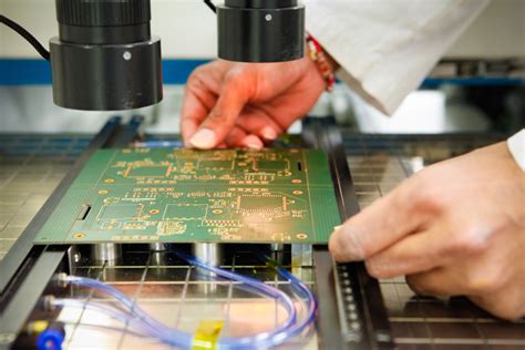
Quality control and testing
After assembly, the PCB undergoes various quality control and testing procedures to ensure proper functionality and reliability, such as:
- Visual inspection for solder joint quality and component placement
- Automated Optical Inspection (AOI) for detecting assembly defects
- In-Circuit Testing (ICT) for verifying the correctness of the assembled components and their connections
- Functional testing to ensure the PCB performs as intended in its final application

PCB Manufacturing Considerations
Material selection
Choose the appropriate PCB material based on your application’s requirements, such as:
- FR-4: A common, cost-effective material suitable for most applications
- High-frequency laminates: Materials with low dielectric loss for high-frequency applications
- Metal core PCBs: PCBs with a metal core for improved thermal management
Layer stack-up
Determine the number of layers needed for your PCB based on the complexity of your circuit and the required signal integrity. Common layer stack-ups include:
- Single-layer: One conductive layer, typically used for simple circuits
- Double-layer: Two conductive layers, one on each side of the substrate
- Multi-layer: Three or more conductive layers, with insulating layers in between, for complex circuits and improved signal integrity
Manufacturing cost optimization
To minimize PCB manufacturing costs, consider the following:
- Panelization: Combine multiple PCB designs onto a single panel to reduce manufacturing time and cost
- Standardized sizes: Use standard PCB sizes to avoid custom tooling fees
- Minimize the number of layers: Fewer layers generally result in lower manufacturing costs
- Avoid tight tolerances: Specify looser tolerances where possible to reduce manufacturing complexity and cost

Finding a PCB Manufacturer
Factors to consider when choosing a manufacturer
When selecting a PCB manufacturer, consider the following factors:
- Manufacturing capabilities: Ensure the manufacturer can meet your PCB’s requirements, such as layer count, material, and surface finish
- Quality standards: Look for manufacturers with quality certifications, such as ISO 9001 or IPC standards
- Lead time: Consider the manufacturer’s lead time to ensure it meets your project timeline
- Cost: Compare quotes from multiple manufacturers to find the best value for your project
- Customer support: Choose a manufacturer with responsive and helpful customer support
Online PCB prototyping services
For low-volume prototypes or small-scale production, online PCB prototyping services can be a convenient and cost-effective option. Some popular services include:
- PCBWay: https://www.pcbway.com/
- JLCPCB: https://jlcpcb.com/
- OSH Park: https://oshpark.com/
- Seeed Studio: https://www.seeedstudio.com/fusion_pcb.html
These services often provide instant quotes, online design rule checks, and quick turnaround times.
Conclusion
PCB manufacturing is a critical process in the creation of modern electronic devices. By understanding the design, fabrication, and assembly processes, you can create reliable and cost-effective PCBs for your projects. Remember to follow design guidelines, choose the appropriate materials and manufacturers, and perform thorough quality control and testing to ensure the success of your PCB-based projects.
Frequently Asked Questions (FAQ)
- What is the minimum trace width and spacing for a PCB?
-
The minimum trace width and spacing depend on the PCB manufacturer’s capabilities and the specific design requirements. Generally, a minimum trace width and spacing of 0.2 mm is achievable by most manufacturers.
-
What is the difference between through-hole and surface-mount assembly?
-
Through-hole assembly involves inserting component leads through holes in the PCB and soldering them on the opposite side, while surface-mount assembly involves placing components directly on the pads and soldering them using a reflow oven or wave soldering machine.
-
What is the purpose of a solder mask on a PCB?
-
A solder mask is a protective layer applied to the PCB that covers the copper traces, leaving only the exposed pads for soldering. It helps prevent solder bridges, protects the traces from oxidation, and provides electrical insulation.
-
How can I reduce the cost of PCB manufacturing?
-
To reduce PCB manufacturing costs, consider panelization, using standardized sizes, minimizing the number of layers, and avoiding tight tolerances where possible. Additionally, comparing quotes from multiple manufacturers can help you find the best value for your project.
-
What are the common file formats required for PCB manufacturing?
- The most common file formats required for PCB manufacturing include Gerber files for each layer of the PCB, drill files for holes and vias, a Bill of Materials (BOM) for component procurement, and assembly drawings for component placement.


Leave a Reply