Introduction
Soldering PCB Boards is a crucial process in the manufacturing of electronic devices. However, even with the most skilled technicians and advanced equipment, defects can still occur during the soldering process. These defects can lead to malfunctions, reduced performance, and even complete failure of the electronic device. Therefore, it is essential to have effective methods for checking and identifying Soldering PCB Defects to ensure the quality and reliability of the final product.
In this article, we will discuss 10 helpful ways to check for defects on soldering PCB Boards. We will cover various techniques, tools, and best practices that can help you identify and resolve common soldering issues, such as bridging, cold joints, and insufficient solder. By implementing these methods, you can improve the quality of your soldering work and reduce the risk of defects in your electronic devices.
1. Visual Inspection
Importance of Visual Inspection
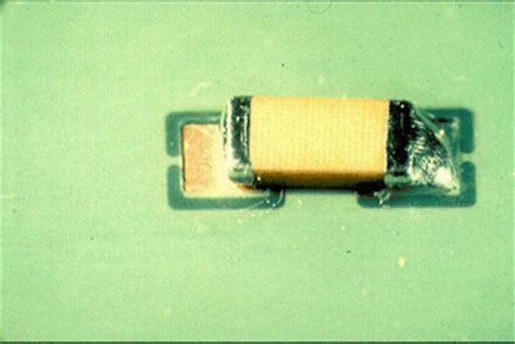
Visual inspection is the most basic and essential method for checking soldering PCB defects. It involves carefully examining the soldered joints and components on the PCB board with the naked eye or using magnification tools. Visual inspection can help identify a wide range of defects, such as:
- Bridging: When solder inadvertently connects two or more pins or pads that should not be connected.
- Cold joints: When the solder joint appears dull, grainy, or has a rough surface due to insufficient heat during soldering.
- Insufficient solder: When there is not enough solder to create a strong and reliable connection between the component and the PCB pad.
- Excess solder: When there is too much solder on the joint, which can cause short circuits or impede the proper functioning of the component.
- Component misalignment: When the component is not properly aligned with the PCB pads, leading to poor connections or mechanical stress.
Tools for Visual Inspection
To perform an effective visual inspection, you may need the following tools:
- Magnifying glass or loupe: A handheld magnifying device that allows you to view the soldered joints in greater detail. Look for a magnification power of at least 10x.
- Microscope: For more detailed inspections, a digital or optical microscope can provide higher magnification (up to 200x) and better image quality.
- Flashlight or task light: Adequate lighting is crucial for spotting defects. Use a bright, focused light source to illuminate the PCB board from various angles.
- Tweezers: Tweezers can be used to gently manipulate components and wires during the inspection process.
Inspection Checklist
When conducting a visual inspection, follow this checklist to ensure you cover all the important aspects:
- Check for bridging between pins or pads.
- Look for cold joints, characterized by a dull, grainy, or rough appearance.
- Verify that there is sufficient solder on each joint, creating a concave fillet between the component lead and the PCB pad.
- Check for excess solder that may cause short circuits or obstruct the component’s functionality.
- Ensure that all components are properly aligned with their respective PCB pads.
- Inspect for any damaged or burnt components, which may indicate overheating during soldering.
- Look for any foreign objects or debris that may have been inadvertently soldered onto the board.

2. X-Ray Inspection
Benefits of X-Ray Inspection
X-ray inspection is a non-destructive testing method that uses X-rays to create images of the internal structure of a soldered PCB board. This technique is particularly useful for detecting defects that are not visible to the naked eye, such as:
- Voids: Small air bubbles trapped within the solder joint, which can weaken the connection and lead to failures.
- Insufficient solder penetration: When the solder does not fully penetrate the plated through-holes (PTHs) or vias, resulting in poor connections.
- Solder balls: Small, spherical solder particles that can cause short circuits if they come into contact with other components or traces.
- Component placement issues: X-ray inspection can reveal if components are misaligned or not properly seated on the PCB pads.
X-ray inspection offers several advantages over visual inspection:
- It can detect defects that are hidden from view, such as those within ball grid array (BGA) packages or under chip components.
- It allows for the inspection of multi-layered PCB boards, as the X-rays can penetrate through the layers to reveal internal defects.
- It provides a permanent record of the inspection results, which can be used for quality control and traceability purposes.
X-Ray Inspection Equipment
To perform X-ray inspection, you will need specialized equipment, such as:
- X-ray machine: A device that generates X-rays and directs them onto the PCB board. The X-rays pass through the board and create an image on a detector or film.
- Image processing software: Software that enhances and analyzes the X-ray images, highlighting potential defects and providing measurements.
X-ray inspection equipment can be costly, so it may not be practical for small-scale or low-volume production. However, many PCB Assembly service providers offer X-ray inspection as part of their quality control process.

3. Automated Optical Inspection (AOI)
How AOI Works
Automated Optical Inspection (AOI) is a computer-based system that uses cameras and image processing software to automatically inspect soldered PCB boards for defects. AOI systems compare the captured images of the PCB board to a predefined set of rules or a reference image of a known good board. Any deviations from the expected results are flagged as potential defects.
AOI systems can detect a wide range of soldering defects, including:
- Bridging
- Insufficient or excess solder
- Cold joints
- Component misalignment
- Missing or incorrect components
The main advantages of AOI are:
- High speed: AOI systems can inspect hundreds of PCB boards per hour, making them suitable for high-volume production.
- Consistency: AOI eliminates the subjectivity and variability associated with human visual inspection, ensuring consistent results.
- Traceability: AOI systems generate reports and store inspection data, which can be used for quality control and process improvement purposes.
AOI System Components
A typical AOI system consists of the following components:
- Cameras: High-resolution cameras capture images of the PCB board from various angles. Some systems use multiple cameras to provide complete coverage of the board.
- Lighting: Proper lighting is essential for accurate image capture. AOI systems often use a combination of front and back lighting to highlight different features of the PCB board.
- Transport mechanism: A conveyor or shuttle system moves the PCB board through the inspection area, ensuring consistent positioning and focus.
- Image processing software: Sophisticated algorithms analyze the captured images, comparing them to the reference data and identifying any discrepancies.
- User interface: A computer display and input devices allow operators to set up the inspection parameters, view results, and manage the AOI system.
Implementing AOI
To implement AOI in your soldering process, follow these steps:
- Define the inspection criteria: Determine which defects you want to detect and establish the acceptable limits for each type of defect.
- Create a reference image: Capture an image of a known good PCB board to serve as a baseline for comparison.
- Set up the AOI system: Configure the cameras, lighting, and transport mechanism to ensure optimal image capture and board positioning.
- Train the system: Teach the AOI software to recognize the features and defects of interest by running a series of sample boards and refining the inspection parameters.
- Run production boards: Once the system is set up and trained, run your production PCB boards through the AOI machine and review the results.
- Analyze and optimize: Use the AOI data to identify trends, pinpoint problem areas, and implement process improvements to reduce defects and increase efficiency.

4. In-Circuit Testing (ICT)
Principles of ICT
In-Circuit Testing (ICT) is a method of testing the functionality and connectivity of individual components on a soldered PCB board. ICT uses a bed-of-nails fixture, which consists of an array of spring-loaded probes that make contact with specific test points on the PCB board. The test points are typically located on the solder pads or vias of the components being tested.
ICT can detect various types of soldering defects, such as:
- Open circuits: When there is no electrical continuity between two points that should be connected.
- Short circuits: When there is an unintended electrical connection between two points that should be isolated.
- Component failures: When a component does not function as expected, either due to a manufacturing defect or damage during the soldering process.
ICT offers several benefits:
- Comprehensive testing: ICT can test a wide range of components, including resistors, capacitors, inductors, diodes, and integrated circuits.
- Speed: ICT systems can test hundreds of points on a PCB board in a matter of seconds, making them suitable for high-volume production.
- Early defect detection: By testing the board at the component level, ICT can identify defects early in the manufacturing process, reducing the cost and time associated with troubleshooting and rework.
ICT Fixture Design
Designing an effective ICT fixture is crucial for accurate and reliable testing. The fixture must provide consistent and stable contact with the test points on the PCB board, while also accommodating any variations in board thickness or component placement.
When designing an ICT fixture, consider the following factors:
- Test point selection: Choose test points that provide access to the critical components and networks on the PCB board. Avoid placing test points too close to sensitive components or high-frequency signals.
- Probe type: Select the appropriate probe type (e.g., spring-loaded, pogo pin, or coax) based on the test point size, spacing, and signal requirements.
- Fixture material: Use a durable and stable material, such as G10 or FR4, for the fixture base to minimize flexing and ensure consistent probe contact.
- Alignment features: Incorporate alignment pins or guides into the fixture design to ensure precise positioning of the PCB board during testing.
- Expansion capability: Allow for future changes or additions to the test coverage by including extra test points or modular fixture design.
Implementing ICT
To implement ICT in your soldering process, follow these steps:
- Define the test requirements: Identify the components and networks that require testing and establish the test parameters (e.g., resistance, capacitance, or voltage thresholds).
- Design the fixture: Create a CAD model of the ICT fixture, including the probe layout and alignment features. Collaborate with the PCB design team to ensure compatibility between the board and the fixture.
- Fabricate the fixture: Manufacture the fixture using a CNC machine or 3D printer, and assemble the probes and wiring harness.
- Develop the test program: Use ICT software to create a test sequence that applies the appropriate stimuli and measures the responses at each test point. Define the pass/fail criteria based on the expected values.
- Debug and validate: Run sample boards through the ICT system to verify the fixture alignment, probe contact, and test coverage. Debug any issues and refine the test program as needed.
- Run production boards: Once the ICT system is validated, run your production PCB boards through the test process and review the results.
- Analyze and optimize: Use the ICT data to identify component failures, process issues, and opportunities for improvement. Work with the manufacturing and engineering teams to implement corrective actions and optimize the soldering process.
5. Boundary Scan Testing
Overview of Boundary Scan Testing
Boundary Scan Testing, also known as JTAG (Joint Test Action Group) testing, is a method of testing the interconnections and functionality of digital components on a soldered PCB board. Boundary Scan uses a special test access port (TAP) built into the components themselves, allowing the test system to control and observe the inputs and outputs of each component without the need for physical access to the pins.
Boundary Scan can detect various types of soldering defects, such as:
- Open circuits: When there is no electrical continuity between two points that should be connected.
- Short circuits: When there is an unintended electrical connection between two points that should be isolated.
- Component failures: When a component does not function as expected, either due to a manufacturing defect or damage during the soldering process.
The main advantages of Boundary Scan testing are:
- Accessibility: Boundary Scan can test components that are difficult or impossible to access with physical probes, such as ball grid array (BGA) packages or chip-scale packages (CSPs).
- Non-intrusive: Boundary Scan does not require physical contact with the component pins, reducing the risk of damage during testing.
- Design for testability: By incorporating Boundary Scan capabilities into the PCB design, you can improve the overall testability and diagnostic capabilities of the board.
Boundary Scan Architecture
To implement Boundary Scan testing, the components on the PCB board must include a Boundary Scan architecture, which consists of the following elements:
- Test Access Port (TAP): A standard interface that allows the test system to communicate with the component’s Boundary Scan logic. The TAP includes four mandatory signals: Test Clock (TCK), Test Mode Select (TMS), Test Data Input (TDI), and Test Data Output (TDO).
- Boundary Scan Cells: Special cells located between each component pin and the internal logic. These cells can capture the state of the pin or force a specific value onto the pin during testing.
- Instruction Register (IR): A register that holds the current Boundary Scan instruction, which determines the mode of operation for the component’s Boundary Scan logic.
- Data Registers (DR): Registers that hold the data being shifted into or out of the component during Boundary Scan testing. The most important data register is the Boundary Scan Register (BSR), which contains the boundary scan cells.
When designing a PCB board for Boundary Scan testing, follow these guidelines:
- Select components that support Boundary Scan: Choose components that include a TAP and Boundary Scan architecture. Many modern digital components, such as FPGAs, CPLDs, and microprocessors, have built-in Boundary Scan capabilities.
- Route the TAP signals: Ensure that the TAP signals (TCK, TMS, TDI, and TDO) are properly routed between the components and the test system. Follow the manufacturer’s guidelines for signal integrity and timing requirements.
- Provide test coverage: Analyze the PCB design to ensure that all critical interconnections and components are accessible via Boundary Scan. Use dedicated test points or vias to provide access to non-Boundary Scan components, if necessary.
Implementing Boundary Scan Testing
To implement Boundary Scan testing in your soldering process, follow these steps:
- Develop the Boundary Scan test program: Use Boundary Scan software to create a test sequence that exercises the interconnections and functionality of the Boundary Scan components. The test program should include a combination of interconnect tests (e.g., open/short detection) and functional tests (e.g., memory read/write).
- Set up the test system: Connect the TAP signals from the PCB board to the Boundary Scan test equipment, such as a JTAG controller or a PC-based tester. Ensure that the test system is properly configured for the specific board and components being tested.
- Run the test program: Execute the Boundary Scan test sequence and monitor the results. The test system will report any failures or discrepancies, along with diagnostic information to help isolate the defect.
- Analyze and debug: Review the test results and use the diagnostic information to identify the root cause of any failures. This may involve visual inspection, additional testing, or collaboration with the design and manufacturing teams.
- Implement corrective actions: Based on the failure analysis, implement appropriate corrective actions, such as process adjustments, design changes, or component replacements, to prevent future defects.
- Re-test and validate: After implementing the corrective actions, re-run the Boundary Scan test to verify that the defects have been resolved and the board is functioning as expected.
6. Flying Probe Testing
Principles of Flying Probe Testing
Flying Probe Testing is a method of testing the connectivity and functionality of a soldered PCB board using movable test probes. Unlike In-Circuit Testing (ICT), which uses a fixed bed-of-nails fixture, Flying Probe Testing uses a small number of probes (typically 4 to 8) that can move independently to any location on the board.
Flying Probe Testing can detect various types of soldering defects, such as:
- Open circuits: When there is no electrical continuity between two points that should be connected.
- Short circuits: When there is an unintended electrical connection between two points that should be isolated.
- Component failures: When a component does not function as expected, either due to a manufacturing defect or damage during the soldering process.
The main advantages of Flying Probe Testing are:
- Flexibility: Flying Probe Testing can accommodate a wide range of board designs and component types without the need for a custom fixture. This makes it ideal for low-volume or prototype production.
- Precision: The movable probes can access small or tightly-spaced test points that may be difficult to reach with a fixed fixture.
- Speed: Modern Flying Probe systems can test a large number of points in a short amount of time, thanks to advanced motion control and test algorithms.
Flying Probe System Components
A typical Flying Probe system consists of the following components:
- Probes: A set of movable test probes, typically mounted on a gantry or robotic arm


Leave a Reply