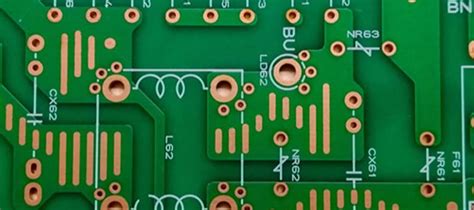
What is a Via in PCB Design?
A via, short for “vertical interconnect access,” is a small hole drilled through a PCB to create an electrical connection between different layers of the board. Vias are typically plated with a conductive material, such as copper, to ensure a reliable electrical connection.
Types of Vias in PCB Design
There are several types of vias used in PCB design, each with its own characteristics and applications:
Through-hole Vias
Through-hole vias are the most common type of via, extending from the top layer to the bottom layer of a PCB. They are used to connect components mounted on both sides of the board and to route signals between layers.
Blind Vias
Blind vias are used to connect an outer layer to an inner layer of a PCB without extending through the entire board. They are typically used in high-density designs to save space and reduce the overall size of the PCB.
Buried Vias
Buried vias are used to connect inner layers of a PCB without extending to the outer layers. They are hidden within the board and are used to create complex routing patterns and improve signal integrity.
Micro Vias
Micro vias are small-diameter vias (typically less than 150 microns) used in high-density PCB designs. They are commonly used in HDI (High-Density Interconnect) PCBs to connect fine-pitch components and create dense routing patterns.
Via Applications in PCB Design
Vias serve several important functions in PCB design:
Interlayer Connection
The primary function of vias is to create electrical connections between different layers of a PCB. This allows designers to route signals and power through the board, connecting components on different layers.
Component Mounting
Through-hole vias are often used to mount through-hole components on a PCB. The component leads are inserted into the via holes and soldered in place, ensuring a secure mechanical and electrical connection.
Thermal Management
Vias can also be used for thermal management in PCB design. Thermal vias are strategically placed near heat-generating components to dissipate heat through the board, preventing overheating and improving the overall reliability of the PCB.
Shielding and Grounding
Vias can be used to create shielding and grounding structures within a PCB. By connecting ground planes and creating via fences, designers can reduce electromagnetic interference (EMI) and improve signal integrity.
Via Design Considerations
When designing vias for a PCB, several factors must be considered to ensure optimal performance and manufacturability:
Via Size and Aspect Ratio
The size of a via is determined by its diameter and the thickness of the PCB. The aspect ratio, which is the ratio of the via’s depth to its diameter, should be kept within manufacturable limits to ensure reliable plating and avoid issues such as voids or incomplete filling.
Via Placement and Spacing
Proper via placement and spacing are crucial for maintaining signal integrity and preventing manufacturing issues. Vias should be placed away from the edges of the board and spaced sufficiently to avoid shorts and ensure reliable plating.
Via Pad Size and Annular Ring
The via pad size and annular ring (the copper area surrounding the via hole) must be designed to accommodate manufacturing tolerances and ensure a reliable connection. The annular ring should be large enough to prevent breakouts and provide sufficient copper for proper plating.
Via Filling and Capping
In some applications, vias may need to be filled or capped to improve reliability, prevent solder wicking, or create a flat surface for component mounting. Various materials, such as epoxy or conductive paste, can be used for via filling, while copper or soldermask can be used for via capping.

Via Manufacturing Process
The manufacturing process for vias involves several steps:
- Drilling: Via holes are drilled through the PCB using a specialized drilling machine.
- Desmearing: The drilled holes are cleaned and the resin smear is removed to ensure proper plating adhesion.
- Plating: The via holes are plated with a conductive material, typically copper, to create an electrical connection between layers.
- Filling/Capping (optional): If required, the vias are filled or capped using the appropriate materials and processes.

Frequently Asked Questions (FAQ)
1. What is the difference between a through-hole via and a blind via?
A through-hole via extends from the top layer to the bottom layer of a PCB, while a blind via connects an outer layer to an inner layer without extending through the entire board.
2. What is the purpose of micro vias in PCB design?
Micro vias are used in high-density PCB designs to connect fine-pitch components and create dense routing patterns. They are commonly found in HDI (High-Density Interconnect) PCBs.
3. How do vias help with thermal management in PCBs?
Thermal vias are strategically placed near heat-generating components to dissipate heat through the board, preventing overheating and improving the overall reliability of the PCB.
4. What factors should be considered when designing vias for a PCB?
When designing vias, factors such as via size and aspect ratio, placement and spacing, pad size and annular ring, and filling or capping requirements should be considered to ensure optimal performance and manufacturability.
5. What is the purpose of via filling or capping?
Via filling or capping is used to improve reliability, prevent solder wicking, or create a flat surface for component mounting. Various materials, such as epoxy, conductive paste, copper, or soldermask, can be used for via filling or capping.

Conclusion
Vias are an essential component of PCB design, allowing for the creation of electrical connections between layers, component mounting, thermal management, and shielding. By understanding the different types of vias, their applications, and design considerations, PCB designers can create reliable, high-performance boards that meet the demands of modern electronics. As PCB technology continues to advance, the role of vias in enabling dense, complex designs will only become more critical.
| Via Type | Description | Application |
|---|---|---|
| Through-hole Via | Extends from top to bottom layer | Connecting components on both sides, routing signals between layers |
| Blind Via | Connects outer layer to inner layer | High-density designs, saving space |
| Buried Via | Connects inner layers | Complex routing, improving signal integrity |
| Micro Via | Small-diameter via (< 150 μm) | High-density designs, connecting fine-pitch components |
In summary, vias are a fundamental aspect of PCB design, enabling the creation of complex, multi-layer boards that power our modern electronic devices. By carefully considering via types, applications, and design factors, PCB designers can ensure the optimal performance, reliability, and manufacturability of their designs.


Leave a Reply